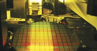
Samsung Electronics plans to invest additional $9.2 billion in capacity expansion of the world’s largest semiconductor fab, a media report claims. At present it is unclear how exactly Samsung plans to expand its fab, but the cost of the whole project – around $23.6 billion – already looks staggering. Samsung …
Read More »ASML sells 15 EUV lithography scanners, possibly, to Intel
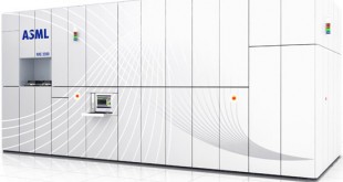
ASML Holding NV, one of the world’s leading makers of semiconductor manufacturing equipment, this week said that it had signed an agreement with one of its major U.S.-based customers to deliver at least 15 ASML extreme ultraviolet (EUV) EUV lithography systems. Given the scale of the order it is highly likely …
Read More »Intel: Transitions to thinner process tech will get harder
Although Intel Corp. imagines its future many years down the road and has a solid vision, it admits that going forward it will be much harder to achieve certain goals as manufacturing technologies get much more complex. Like other huge companies, Intel Corp. has big plans for the future. Recently …
Read More »Intel: We will not need EUV for 10nm process technology
Intel Corp. officially confirmed on Wednesday that it will not use extreme ultraviolet (EUV) lithography for its 10nm process technology allegedly due to come online in 2016. Apparently, not only the EUV scanners are not ready, but backbones of certain fabs may not support the new equipment due to its …
Read More »TSMC extends 28nm chip lead time to 16 weeks, puts chip designers at risk
Taiwan Semiconductor Manufacturing Co. has extended lead time for production of chips using 28nm process technology from ten to 16 weeks recently, a media report reads. The company reportedly claimed that the demand for 28nm manufacturing process is very high and therefore orders placed in May would take more time …
Read More »TSMC reveals new 16nm FinFET+ process, vows to start 10nm production in Q4 2015
Taiwan Semiconductor Manufacturing Co. this week unveiled an improved version of its 16nm FinFET process technology that will hit volume production in 2015. In addition, the company revealed some details regarding its 10nm FinFET fabrication process and said that it would start risk production using the technology in Q4 2015, …
Read More »Intel remains committed to 450mm wafers, but there will be a delay
Early last year Intel Corp. demonstrated the world’s first fully-patterned 450mm wafers and in mid-2013 started to construct D1X module 2 fab, which is supposed to act as a primary development facility for virtually all of Intel’s 450mm initiatives. It was expected that commercial production of chips on 450mm wafers …
Read More »nVidia not satisfied with 12″ – Jen Hsun wants more
When all nVidia did was graphic chips for graphic cards, there was always a decent amount of production capacity available in the world. Now that it's busy pioneering in the phone sector – the numbers have caught Jen Hsun's gang out. They need more and they're gasping for it. KitGuru …
Read More » KitGuru KitGuru.net – Tech News | Hardware News | Hardware Reviews | IOS | Mobile | Gaming | Graphics Cards


