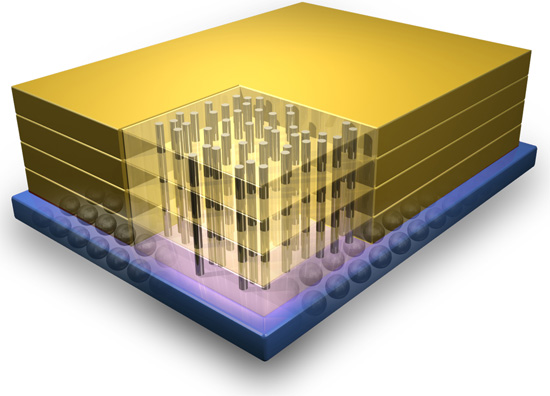
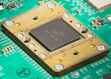
Micron Technology is working on the third generation of its hybrid memory cube technology, which will be unveiled next year. If the third-gen HMC doubles data rate of the memory from 15Gb/s today, then the new memory technology will offer unprecedented bandwidth.
HMC uses advanced through-silicon vias (TSVs) – vertical conduits that electrically connect a stack of individual chips – to combine Micron’s high-performance logic with Micron's dynamic random access memory. At present Micron offers 2GB and 4GB HMC devices based on 4Gb DRAM dies with up to 15Gb/s data-rates and up to 160GB/s peak bandwidth per device.
At present, Micron is working on next-generation HMC, which could improve density and bandwidth, reports HPC Wire. Nothing particular is known about the third-gen HMC, but it is logical to expect Micron to improve performance and capacity of HMC.
“To be frank, we cannot achieve the applications and system needs without developing a really good packaging technology,” said Scott Graham, Micron’s general manager of Hybrid Memory at the Intel Developer Forum last month. “We’re not going to achieve these bandwidth capabilities. We’re not going to achieve the reliability needs. We’re not going to overcome some of the scaling challenges without developing some of these new technology methods. If you look at Hybrid Memory Cube, that’s been the lead vehicle for Micron in order to develop these package technologies for future emerging memories.”
HMC is supported by various special-purpose microprocessors. In addition, HMC will be used by Intel’s next-generation Xeon Phi co-processor code-named “Knights Landing”. HMC competes against high-bandwidth memory (HBM), but is based on different principles. Instead of using ultra-wide interface, HMC features up to 16-bit serial interconnect operating at a very high clock-rate. Maximum bandwidth supported by one HBM chip is up to 128GB/s, but second-generation HBM will have bandwidth of up to 256GB/s.
“If we have the ability to take DRAM and stack it on top of a logic layer and SoC and be able to control that DRAM with that SoC, it allows us to overcome scaling challenges,” said Mr. Graham. “Being able to combine these technologies together, gives us unprecedented memory bandwidth that keeps pace with multiple CPU cores, and DRAM alone is not going to do that. This all allows for increased savings in energy/bit, density in a small form factor, higher performance and lower energy, and compelling RAS features.”
Discuss on our Facebook page, HERE.
KitGuru Says: HMC makes a great business sense for Micron, who is the only producer of such memory and can control pricing. However, for developers of bandwidth-demanding applications it makes a lot of sense to use HBM instead of HMC because of pricing concerns. HMC has a number of advantages over HBM, but for those, who do not need features like RAS, its advantages are not important. The arrival of HBM will affect popularity of HMC.
 KitGuru KitGuru.net – Tech News | Hardware News | Hardware Reviews | IOS | Mobile | Gaming | Graphics Cards


i choose HBM over HMC
What ever happened to the HMC Consortium and the other suppliers who were going to make this? Oh yea, they are making HBM now.