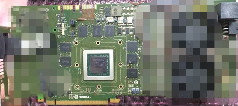
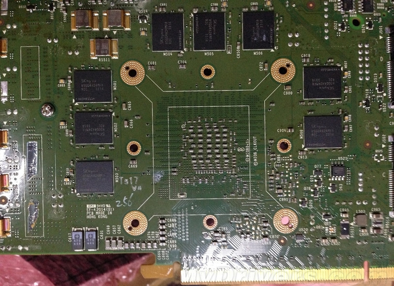
A Chinese web-site on Wednesday published images of an unknown Nvidia graphics card that carries a chip that is only several weeks old. It is believed that the graphics adapter is based on the code-named GM104/GM204 graphics processing unit powered by the Maxwell architecture. The graphics board is expected to become commercially available under the GeForce GTX 880 name.
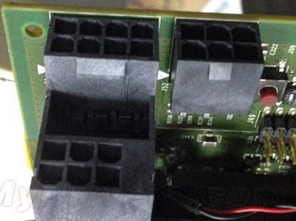
The picture of the graphics adapter that was published by MyDrivers is heavily masked in order to protect identity of the source and therefore we have no idea about peculiarities of the graphics card’s design. What we do know from the images of the graphics board is that it is a high-end solution that carries a lot of memory, requires up to 375W of power (it has two 6-pin and one 8-pin PCIe power connectors) and supports 3-way/4-way SLI technology. The board is not the final since it features a number of technical connectors and knobs not present on commercial products (it is also hard to believe that a single-GPU graphics card needs 375W of power), which is an indicator that the graphics adapter is months away.
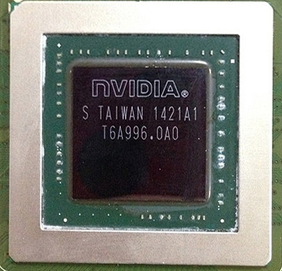
The mysterious graphics card is powered by the A1 revision an unknown graphics processing unit (marked as 1421A1 T6A996.0A0), which was made on the 21st week of the year 2014 (in late May). The chip itself is about the size of the code-named GK104 GPU, maybe a little bigger, but definitely not as big as the code-named GK110 graphics processor. The die size of approximately 300mm2 indicates that the chip is a new performance-mainstream GPU from Nvidia. Previously it was reported that the codename of the chip is either the GM104 or the GM204.
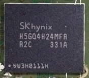
The graphics card carries 16 GDDR5 memory chips from SK Hynix marked as H5GQ4H24MFR-R2C. The memory ICs feature 4Gb density and can operate at up to 7.0GHz effective data-rate. Such memory has been on the market for some time now. 16 GDDR5 chips with 4Gb density provide 8GB of memory.
Nowadays high-end graphics cards from Nvidia carry 3GB or 6GB of memory. It is logical to assume that the company’s next-generation graphics solutions will feature 8GB of memory. What is unclear is whether the new GPU features 256-bit or 512-bit memory bus. Usage of high-end GDDR5 as well as the fact that the GM104/GM204 GPU is not the top-of-the-range chip imply that the 256-bit bus is used. 7GHz GDDR5 memory could provide sufficient amount of bandwidth for the graphics processor.
Traditionally, graphics chip designers use A2 revisions of their chips on commercial versions of graphics cards. Assuming that Nvidia got the A1 revision of the GM104/GM204 in late May and that it takes several months to prep a new version of the GPU, if everything goes well the company will get the final A2 revision in August or September. The company may start mass production of the new graphics processor once it ensures that the A2 works well and launch the GM104/GM204 commercially late this year.
Nvidia did not comment on the news-story.
Discuss on our Facebook page, HERE.
KitGuru Says: While it is now clear that Nvidia already has its new high-performance GPU at hands, specifications of the chip as well as manufacturing technology used to make it remain completely unknown.
 KitGuru KitGuru.net – Tech News | Hardware News | Hardware Reviews | IOS | Mobile | Gaming | Graphics Cards


ALIENS
i think that in the final version you’ll only need a 6+8 pin power connector and the extra 6 pin is for development purposes