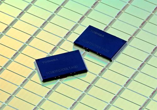
SanDisk Corp. said that it is on-track to ship NAND flash memory produced using 15nm fabrication process this quarter. The company will expand production using 15nm process technology in 2015. SanDisk believes that such memory will be considerably cheaper compared to NAND produced by other makers.
“We are on track to begin product shipments of 15nm this quarter, with meaningful production in Q1 of 2015,” said Sanjay Mehrotra, chief executive officer of SanDisk, during a conference call with investors and financial analysts last week. “We believe our 15nm technology node, using both X2 (MLC – KitGuru) and X3 (TLC – KitGuru) architectures, will be the lowest cost memory technology in the industry in 2015, with capability to serve all product apps, ranging from consumer to enterprise.”
It is interesting to note that Toshiba announced 15nm NAND flash back in April. Apparently, actual mass production of memory using 15nm process technology started only recently…
While NAND flash made using thinner process technologies tends to be cheaper than NAND flash made using thicker fabrication processes, it should be noted that it also features lower write endurance. For example, if multi-level cell NAND flash made using 40nm-class process could sustain around 10000 program-erase cycles, then modern MLC NAND can sustain only around 3000 P/E cycles. Endurance of SanDisk’s 15nm NAND flash is unclear.
Since SanDisk co-owns NAND flash production facilities with Toshiba, it is logical to expect the latter to also start shipping 15nm NAND flash to its partners this year. For example, OCZ, which is owned by Toshiba, could launch SSDs based on the new memory early in 2015.
The Q4 of SanDisk’s fiscal year corresponds to the fourth calendar quarter.
Discuss on our Facebook page, HERE.
KitGuru Says: It will be interesting to see how durable will TLC NAND flash memory made using 15nm technology be. Will it endure 1000 P/E cycles like modern TLC, or will it become even less durable?
 KitGuru KitGuru.net – Tech News | Hardware News | Hardware Reviews | IOS | Mobile | Gaming | Graphics Cards


