Advanced Micro Devices will reveal all technical details about its next-generation code-named “Carrizo” accelerated processing unit in late February, 2015, at the 2015 IEEE international Solid-State Circuits Conference (ISSCC). Although many things about the chip are already known, AMD managed to create an intrigue by squeezing in 28 per cent more transistors without changing process technology or increasing die size.
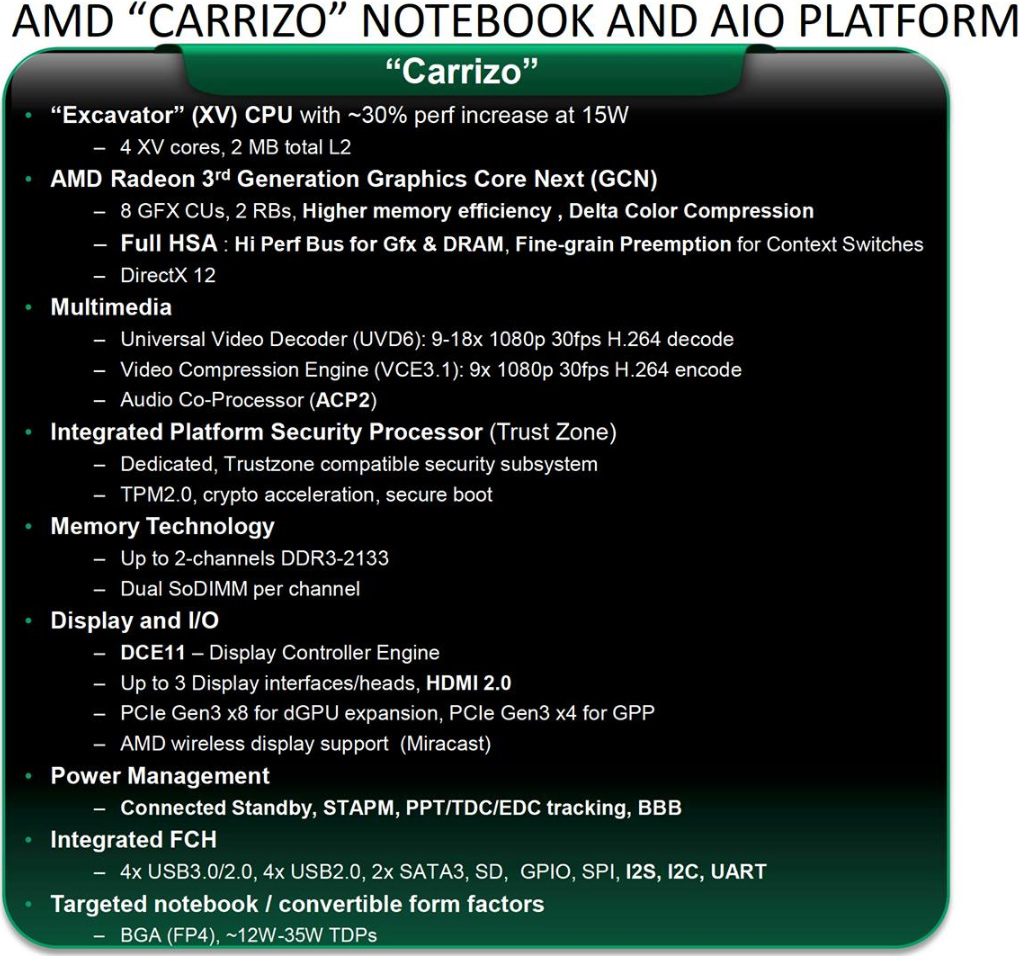
Based on unofficial information, AMD “Carrizo” accelerated processing unit packs two dual-core AMD “Excavator” (XV) modules, AMD Radeon graphics based on third iteration graphics core next architecture (GCN 1.2) with eight compute units (512 stream processors in total), an integrated dual-channel DDR3 memory controller, a new special high-performance bus to connect x86 cores to graphics cores and DRAM, additional HSA [heterogeneous system architecture] enhancements, PCI Express 3.0 controller as well as all-new multimedia and input/output engines.
According to AMD’s description of the “Carrizo” silicon it plans to describe at the ISSCC, the chip will be made using 28nm process technology. Surprisingly, the APU will integrate 3.1 billion of transistors, 28 per cent more compared to the current-generation “Kaveri” APU, but maintain rather small die size of 244.62mm2 (Kaveri is 245mm2).
It is unclear how AMD managed to squeeze in 28 per cent more transistor into a chip made using a similar 28nm process technology without increasing its die size. Perhaps, AMD will use another 28nm fabrication process either from GlobalFoundries or from Taiwan Semiconductor Manufacturing Co. that has higher transistor density than GF’s 28SHP manufacturing technology.
AMD plans to formally introduce its “Carrizo” APU in the first half of 2015.
Discuss on our Facebook page, HERE.
KitGuru Says: It is rather surprising that AMD’s “Carrizo” APU will be considerably more complex than the company’s “Kaveri” chip. If AMD does not sacrifice clock-rate for transistor density and die size, then expect Excavator-based chips to be noteworthy better than the existing “Kaveri” A-series APUs.
 KitGuru KitGuru.net – Tech News | Hardware News | Hardware Reviews | IOS | Mobile | Gaming | Graphics Cards


Bought a 860K while waiting for Carrizo. Can’t wait to see how Carrizo comes out to be.
They use gpu libraries of transistors and design procedures when track the circuits, thats why more dense result
Many of you dont really need to buy Intel chips, so please use AMD instead!!
I’m quite interested in the 860K but reviews are very few and far between. How do you like it? And how do you suppose it would compare to, say, an FX-4350?