Taiwan Semiconductor Manufacturing Co. has ordered two additional extreme ultraviolet (EUV) lithography scanners from ASML Holding. The equipment will be delivered in 2015 and will complement initial two EUV scanners TSMC has today, which will be upgraded. Four scanners will let TSMC make chips using 10nm process technology and EUV lithography tech in commercial quantities.
Next year ASML will deliver two NXE:3350B EUV systems to TSMC. In addition, ASML will upgrade TSMC’s existing NXE:3300B systems with new light sources that will increase their production capacity to the levels of NXE:3350B, which will allow the world’s largest contract maker of semiconductors to start volume commercial production of 10nm chips using EUV lithography equipment sometimes in 2016 – 2017.
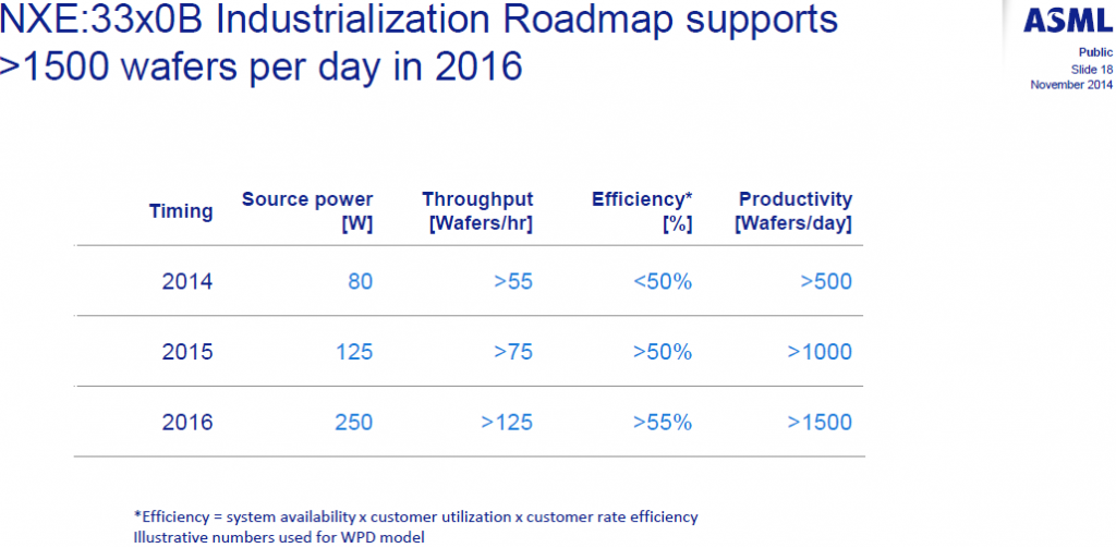
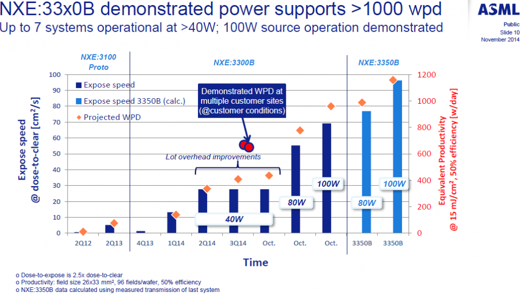
At present ASML’s NXE:3300B scanners – which are installed at various semiconductor manufacturing facilities across the world – feature 80W light sources and can process about or over 500 wafers per day. Sometimes next year ASML will have 125W light sources for the NXE:3300B and the NXE:3350B systems, which will boost their productivity to 1000+ wafers per day, which may be nearly enough to start commercial usage. In 2016 the company plans to supply 250W light sources that will further increase productivity to 1500 wafers per day.

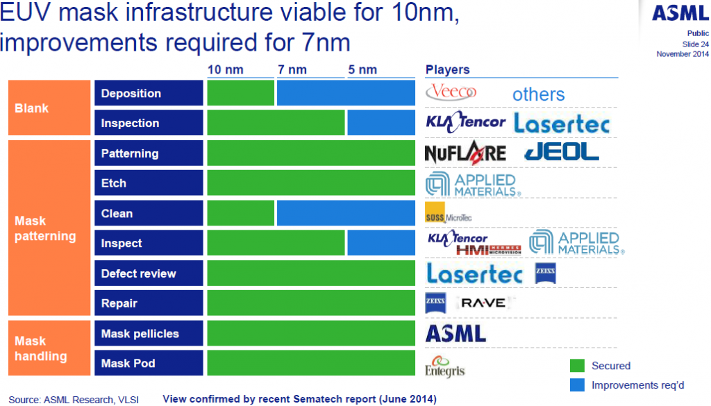
While ASML itself has a solid roadmap for EUV equipment in place and everything depends on whether it can deliver more powerful light sources on time, other companies are only ready with EUV infrastructure acceptable for 10nm node. Improvements are required for volume production at 7nm node. Meanwhile, Intel Corp. and, apparently, some other big players, only plan to adopt EUV at 7nm.

Discuss on our Facebook page, HERE.
KitGuru Says: With four EUV scanners installed, TSMC will clearly make the majority of its 10nm chips using EUV lithography, which may provide it a lot of benefits compared to other foundries, if all goes well. But what if it does not?
 KitGuru KitGuru.net – Tech News | Hardware News | Hardware Reviews | IOS | Mobile | Gaming | Graphics Cards


