Late last year Advanced Micro Devices said that it would use 20nm fabrication technology offered by Taiwan Semiconductor Manufacturing Co., but only for for select products. According to AMD’s recent filing with the Security and Exchange Commission, the company has not yet started to use the 20nm manufacturing process.
AMD uses GlobalFoundries and TSMC as exclusive manufacturers of its chips. GlobalFoundries produces a variety of accelerated processing units, central processing units, graphics processing units and semi-custom chips for video game consoles using 28nm and 32nm fabrication technologies, the company disclosed in a recently released form-10K. TSMC makes APUs, GPUs and chipsets for AMD using various manufacturing processes ranging from 28nm to 65nm. The chip designer made no disclosures regarding its usage of TSMC's 20nm process.
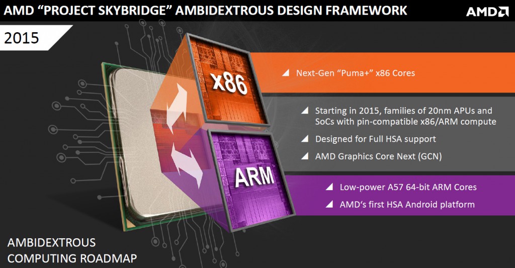
AMD has not revealed the whole lineup of chips it plans to make using 20nm fabrication process at TSMC. Officially, the company indicated that it would use 20nm manufacturing tech for its project “Skybridge” processors code-named “Amur” (featuring ARMv8-A cores) and “Nolan” (featuring Puma+ x86 cores). Besides, it is known that the company plans to use 20nm for low-cost version of Xbox One system-on-chip. It is also possible that AMD will build an inexpensive version of PlayStation 4 SoC as well as a low-power graphics processing unit using the tech.
Typically production of chips starts several months before formal introduction. Since as of late February AMD has not started to produce anything at 20nm node, it is clear that all 20nm chips from the company will be available only in the second half of the year. This also proves that all new graphics processing units that AMD plans to introduce in mid-2015 will be made using 28nm high-performance fabrication process.

TSMC’s 20nm manufacturing process was designed for low-power mobile system-on-chips for smartphones and tablets. At present it is used by Apple, Qualcomm and some other customers of the world’s largest contract maker of semiconductors.
Discuss on our Facebook page, HERE.
KitGuru Says: There are rumours that AMD intends to keep using 28nm manufacturing technology for its Nolan accelerated processing units. If they are true, it may mean two things: TSMC’s 20nm process tech is completely unsuitable for anything complex and custom; AMD’s project Skybridge in its current form has failed because the main idea of the initiative is to create similar pin-to-pin compatible 20nm chips with either ARM or x86 cores.
 KitGuru KitGuru.net – Tech News | Hardware News | Hardware Reviews | IOS | Mobile | Gaming | Graphics Cards


I’ll happily stick with my R9 290 till at least 2016 then!
The collaboration with Mediatek can be a very good reason to abandon the earliest roadmaps and just concentrate into getting the GCN architecture into Mediatek chips. After that Mediatek can take over the ARM designs completely and AMD just help them to create some more powerful designs for laptops, chromebooks, desktops and servers.
TSMC seems to be having issues with 20nm. How sure are we that their 16/14nm will be on time for Zen?
Nolan is GF20LPM. It is a known thing not much of a secret since the design world is not that big, word gets around.