

Taiwan Semiconductor Manufacturing Co. believes that its 10nm fabrication process will not only be available around the same time when Intel Corp. starts to use its 10nm technology, but will also offer similar performance and density as Intel’s.
In a bid to speed up time-to-market of their manufacturing processes featuring FinFET transistors, leading contract makers of semiconductors had to mix multi-gate transistors with back-end-of-line (BEOL) interconnect flows of their 20nm manufacturing technologies. As a result, while TSMC, GlobalFoundries and Samsung Electronics formally offer their customers 14nm and 16nm FinFET processes, which can speed up various chips or cut down their power consumption, they only offer chip geometries comparable to those of products made using 20nm technologies. By contrast, Intel has “true” 14nm fabrication tech and can benefit from smaller CPU sizes and costs. With 10nm TSMC will move on to 10nm BEOL interconnects and thus will give its customers an opportunity to shrink their chips.
“The performance of our 10nm, in terms of speed, power and density will be equal to what we believe Intel will define as its 10nm technology,” said Elizabeth Sun, TSMC Director of Corporate Communications, in an interview with EE Times. “Technology-wise, we think we can close the gap at 10nm.”
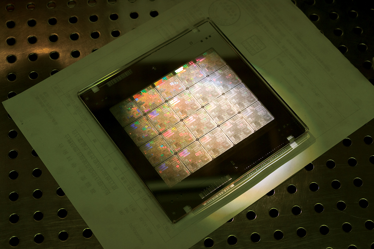
According to TSMC’s predictions, its 10nm FinFET will offer over 25 per cent clock-rate improvement over the 16nm FinFET+ at the same power, it is projected to be 45 per cent more energy efficient and is predicted to provide 2.2 times higher density over 16nm FinFET+, which is a massive improvement. Risk production of 10nm FinFET chips is scheduled to start in the fourth quarter of 2015, whereas high-volume manufacturing will begin in 2017.
As reported, TSMC will use both immersion as well as extreme ultraviolet (EUV) lithography tools for 10nm production. The company yet has to provide precise details how it plans to use EUV. The use of EUV for process technology beyond 10nm still depends on whether it will be ready for manufacturing.
“We are working with ASML with the objective at some future point if extreme ultraviolet (EUV) becomes manufacturing ready, we can insert EUV partially to 10nm,” said Ms. Sun. “Partial insertion means only in a few critical layers. It is still a work in progress.”
TSMC has been aggressively increasing spending on research and development and manufacturing capacity expansion in the recent years. This should help the company to offer manufacturing technologies comparable to those used by Intel to make its microprocessors.
Discuss on our Facebook page, HERE.
KitGuru Says: It is interesting that TSMC does not compare itself with other foundries anymore, but prefers to compare itself against Intel, which has not yet become a major contract maker of semiconductors.
…
Can someone explainto me why 16nm was such as struggle with yeilds but 14nm and apparantly 10nm wasn’t?
Because they didn’t have their Fab tech matured. When you get that small you increase the risk and start to encounter leakage. They needed to get their process down to the point of a more than acceptable rate of failure caused by this.
He asked about 16nm specifically.
I gave an appropriate response to his question…
…which could be said for any xxnm process.
Except they’re talking about how they need to work on these for the lower NM since they did not work it through the 16nm process right the first time. A lessons learned that they are going to apply to the lower NM fabrications.
http://wccftech.com/tsmcs-16nm-finfet-faces-delays-qualcomm-jumps-ship-samsung/
Ok i get it.
TSMC’s 16FF process is now an entire year behind the original schedule promised by the company. To make matters even worse Qualcomm has reportedly cancelled it’s trial risk production at the Taiwanese fab due to the low capacity and poor yields. In turn Samsung has reduced pricing, increased production capacity and achieved a new yield breakthrough for its 14nm FinFET process. And this is what prompted Qualcomm to finally decide to jump ship.
A buddy of mine doing logistics for TSMC said they are purchasing supplies already to replace silicon and test them. They’ve got 3 options before them and the yields and cost of production will likely decide the winner of their 7NM and 5NM process. From there they’re looking at Graphine solutions to be more mature.
What’s the word going around TSMC, or your take on the Samsung/GloFlo collaboration?
You mean GloFo? I don’t know, the collaboration is more or less a request to better efforts in creating low cost mass production. More so to AMD’s advantage since they’re behind in the game and Samsung has shared interests. I wouldn’t be surprised if we see a buyout down the road from Samsung.
No, Samsung and GloFlo are sharing technologies, leaving TSMC to fend for themselves.
http://wccftech.com/samsung-globalfoundries-tsmc-finfet-production/
Right, but it’s Global Foundries not Global Floundries… Lol
lol ooops.
I was under the impression that graphene was only usable in analog devices. Would be interesting to find out how they overcame that problem.