SK Hynix is about to announce new multi-level cell (MLC) NAND flash memory chips that are expected to boost performance of solid-state drives in various applications. The new chips also promise better reliability than previous-generation NAND flash ICs [integrated circuits].
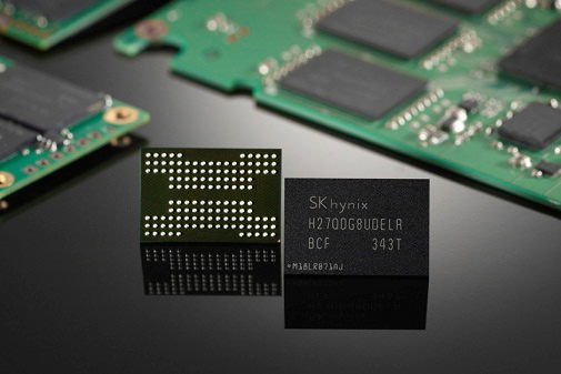
The world’s third largest producer of NAND flash memory is preparing to release the industry’s first multi-level cell (MLC) NAND flash memory chips with 6MB block sizes. Enlarged block sizes could improve performance of solid-state drives based on the new ICs in write-intensive applications, such as servers and content creation. The lineup will consist of 64Gb, 128Gb, 256Gb and 512Gb devices with toggle DDR 2.0 interface (up to 400Mb/s data rate per chip). The chips are to be made using 16nm planar process technology.
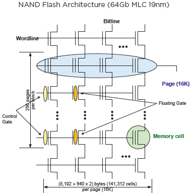
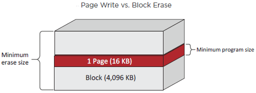
NAND flash memory stores the information in an array of floating-gate transistors (which are called memory cells), with the bit value determined by the amount of charge trapped in the floating gate. Arrays of floating-gate transistors are combined into bit and word lines. Cells located on the same bit line create a page, which is the smallest area of the flash memory that supports a write operation. Multiple pages form a block, which is the smallest area of the flash memory that can be erased in a single operation.

Every write/erase operation causes wear out of NAND flash memory cells. Due to the NAND architecture of sharing bit control lines across multiple storage transistors, erasing a cell necessitates wiping out the entire block, which contains that cell. Moreover, once a defect within a block occurs, SSD controller disables the entire block (assuming that adjacent cells were also affected by the flaw). To minimize the number of block erases and maximize flash memory service life, advanced block management techniques reduce unnecessary erase operations.

In theory, the smaller is the block size, the more durable is flash memory (which is the case for contemporary single-level cell flash memory with block sizes of only 128KB). However, in the real world it means that it gets increasingly hard (and time taking) to erase a huge amount of blocks during data write operations in case of high-capacity multi-level cell (MLC) and triple-level cell (TLC) NAND flash. Typically, MLC and TLC NAND flash block sizes are 2MB or 4MB. The upcoming chips from SK Hynix will be the first MLC NAND flash devices to feature 6MB block sizes.
Since wiping out a group of 6MB blocks takes less time than erasing a greater amount of 4MB blocks, enlarged block sizes will speed up random write operations. The latter are often performed by servers and workstations applications.
However, bigger blocks also mean that SSD makers will have to use sophisticated controllers that “know” how to deal with such blocks and minimize the number of block erases. The fact that SK Hynix decided to produce MLC memory devices with 6MB block sizes means that the company is confident of both modern SSD controllers and improved reliability of its 16nm MLC NAND chips.
At present it is unknown whether SK Hynix plans to sell the new NAND flash memory chips as enterprise-grade eMLC (which is logical, given the main advantages of such memory IC), or as regular MLC. One thing, which is clear, is that the chips are going to be rather unique, at least for now.
Discuss on our Facebook page, HERE.
KitGuru Says: While we do not expect massive (e.g., circa 20 per cent) performance increase from the new memory chips, they will likely power new SSDs with improved random write performance. Moreover, eventually all MLC and TLC NAND flash devices will get increased block sizes.
 KitGuru KitGuru.net – Tech News | Hardware News | Hardware Reviews | IOS | Mobile | Gaming | Graphics Cards


Start earning at home and receive extra check every week… By doing
simple computer-based jobs on your laptop… I do this 3hr every day, 5
days in week and I earn thousand bucks each week…
-> If you are interested in trying this Try it <-