Taiwan Semiconductor Manufacturing Co. has announced that it had produced the first verification chips for its 10nm manufacturing technology. The world’s largest contract maker of semiconductors plans to start risk production using 10nm fabrication process late this year and to initiate high-volume manufacturing in late 2016 or in 2017.
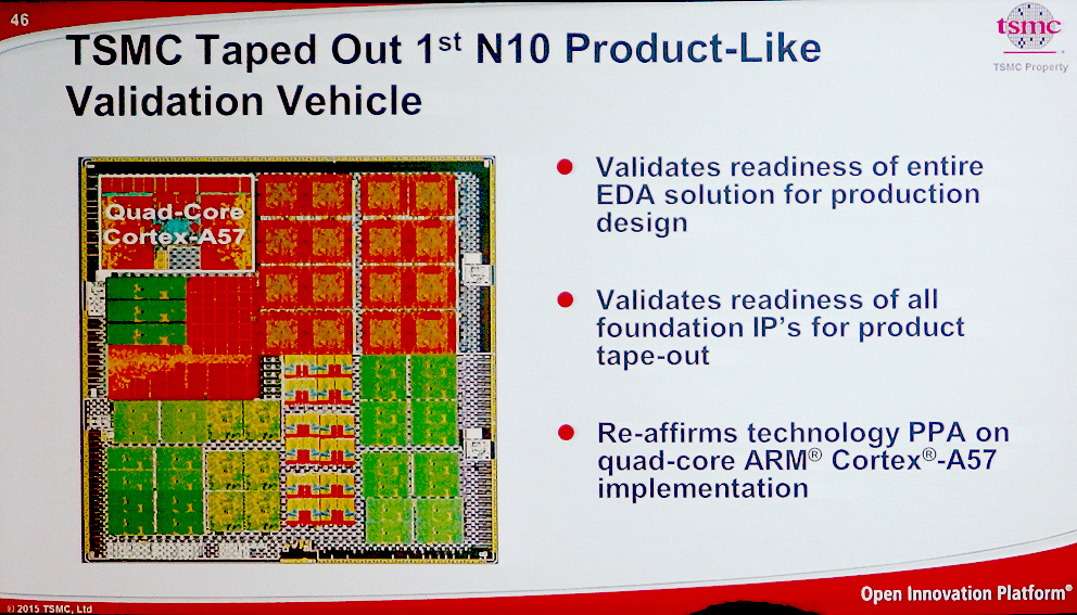
At the 52nd Design Automation Conference in San Francisco, California, TSMC announced that it had successfully taped out and produced its first “product-like” validation vehicle for 10nm manufacturing technology, reports Nikkei BP. Earlier this year the company demonstrated a 300mm wafer processed using its 10nm tech containing SRAM memory. TSMC did not reveal when it produced the validation IC [integrated circuit], but since the symposium took place early last month, it is likely that TSMC got the chip in April or May.
Validation vehicles are needed to make sure that the fabrication process, electronic design automation (EDA) software, interconnect flows, intellectual property and actual building blocks of chips work fine and can be used to design and produce commercial products. Validation vehicles may or may not feature complex chip designs, but they usually contain critical elements of chips. TSMC’s 10nm test IC features a quad-core ARM Cortex-A57 module, which is a clear indicator that the company’s 10nm FinFET (CLN10FF) process technology is ready for design of advanced system-on-chips. TSMC did not reveal any details about its validation vehicle or clock-rate potential of actual SoCs.
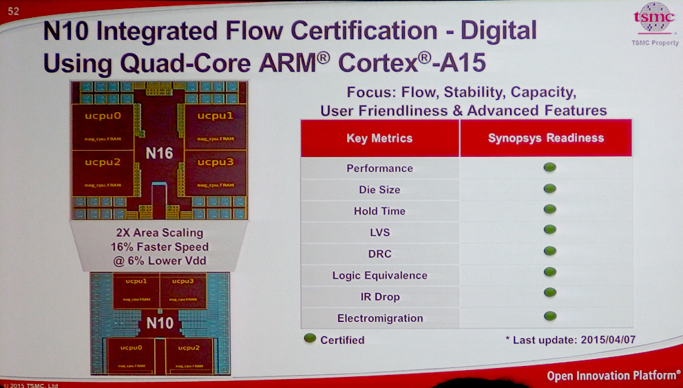
TSMC unveiled the first details regarding its 10nm fabrication technology earlier this year. The company’s 10nm manufacturing process will have 110 per cent higher logic density compared to its 16nm FinFET+ (CLN16FF+) process tech, 20 per cent higher clock-rate potential at the same power and 40 per cent lower power consumption at the same frequency.
Increased transistor density means that per-transistor costs of 10nm chips will be lower than per-transistor costs of 16nm products. Nonetheless, since design of chips with FinFET transistors is generally very expensive and starts at around 80 million for a mainstream SoC, many smaller companies will be unable to utilize either 10nm or 16nm.
TSMC started to construct its 10nm pilot line at its fab 15 phase 5 (pictured, located in Hsinchu Science Park, Taiwan) in June, according to media reports. The pilot line, which will cost TSMC over a billion of dollars, will take several months to complete and then TSMC will start trial production of actual chip designs in late 2015. In Q2 2016 the company is expected to start construction of a brand new fab, which will be dedicated to 10nm manufacturing.
It is interesting to note that TSMC still has plans to introduce a version of 10nm fabrication process that will use extreme ultraviolet (EUV) lithography production tools. Thanks to 13.5nm wavelength of EUV lasers, it will be possible to “draw” finer elements of chips without using tricky multiple-patterning techniques and implementing additional metal layers that complicate production process and make it more expensive. EUV also promises to bring significant benefits in terms of yield and cycle time. Since EUV will eliminate need for multi-patterning during production, design process of chips will get a bit simpler, which will let smaller companies to take advantage of ultra-thin FinFET process technologies.
Samsung Technology has also demonstrated the first 300mm wafers processed using its 10nm manufacturing technology. The company hopes to start high-volume production of semiconductors using 10nm fabrication process in 2016.
Intel Corp. is expected to reveal more details regarding its 10nm plans later this year. Unofficial information points to the fact that the company will not start mass production of its 10nm chips before late 2016. Many believe that Intel will ramp 10nm production only in 2017.
GlobalFoundries has been developing its 10nm fabrication process in-house for a while. Since recently the company completed acquisition of IBM's microelectronics business, it is expected that its 10nm process will rely on technologies developed by engineers from both companies.
Discuss on our Facebook page, HERE.
KitGuru Says: TSMC is clearly on-track for risk production of chips using 10nm technology in late 2015, which means that if everything goes well and yields of actual ICs are fine, we will see the first commercial 10nm system-on-chips in 2017. But will the yields and costs be fine?
 KitGuru KitGuru.net – Tech News | Hardware News | Hardware Reviews | IOS | Mobile | Gaming | Graphics Cards


Meanwhile, AMD and Nvidia are still releasing cards with 28nm chips… I know it isn’t directly relevant but that’s quite a gulf…
Indeed. I feel victim myself; I own a 980 GTX
🙁