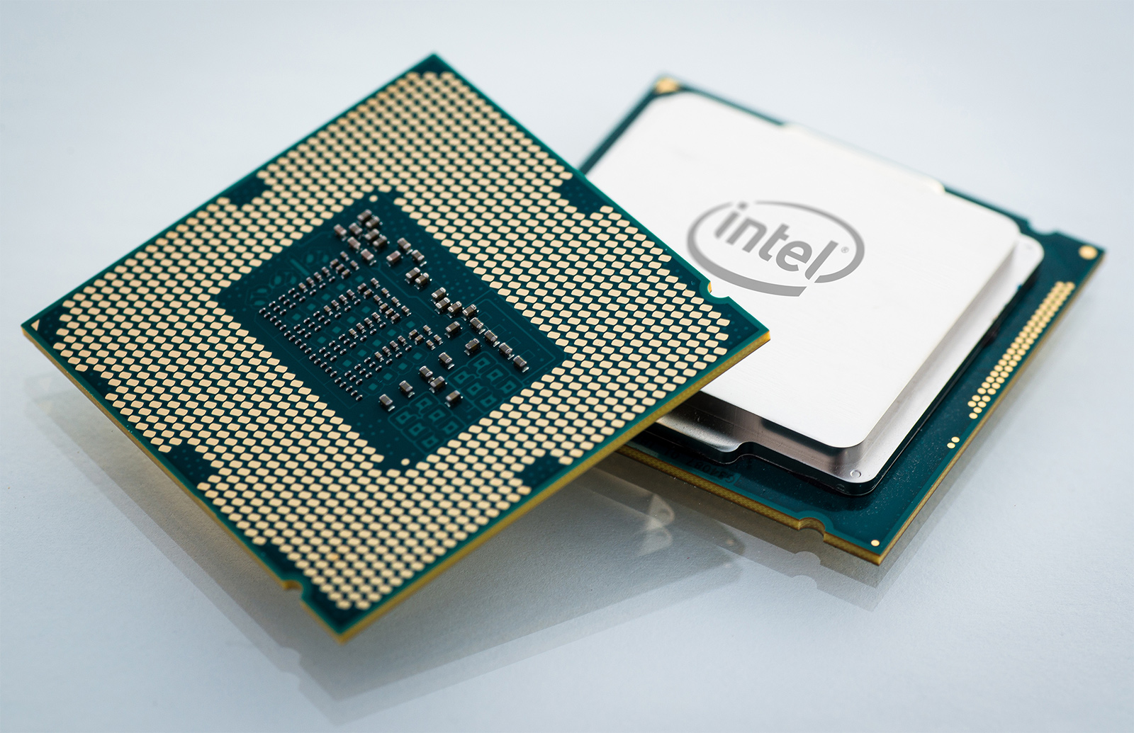
Intel Corp.’s “Kaby Lake” central processing units will be released exactly a year after the company’s “Skylake” chips due this August and September. The introduction of chips in late third quarter means that the company will further postpone the roll-out of microprocessors made using 10nm fabrication process.
As reported, Intel’s “Kaby Lake” processors will replace the company’s “Cannon Lake” central processing units next year and will succeed its “Skylake” products. The chips will be build using 14nm manufacturing technology and will likely resemble “Skylake” both in terms of design and in terms of micro-architecture. It is unknown whether the new CPUs will support any new instructions, such as AVX-512 (AVX 3.2) or any other significant improvements.
Earlier it was believed that the “Kaby Lake” was a temporary solution in order to refresh Intel’s product lineup before all-new 10nm “Cannonlake” chips hit the market, which is something that happened to “Broadwell”. It now appears that the “Kaby Lake” is a product family that will be Intel’s primary product lineup for a long time, according to DigiTimes. The report claims that Intel will start to roll-out the consumer versions of “Kaby Lake” chips in September, 2016, and will conclude the roll-out with high-end enterprise-class “Kaby Lake” processors in early 2017. Such launch schedule indicates that the world’s No. 1 maker of microprocessors will not release its 10nm chips until sometimes in 2017.
Based on what is currently known about the new microprocessors, “Kaby Lake” chips feature two or four cores, a new generation integrated graphics engine, a dual-channel memory controller and up to 256MB of on-package cache to speed-up graphics workloads. Intel’s “Kaby Lake” processors for desktops will retain LGA1151 form-factor and will be drop-in compatible with “Skylake” infrastructure and motherboards powered by Intel’s 100-series chipsets.
Different versions of “Kaby Lake” processors – “Kaby Lake-S”, “Kaby Lake-H”, “Kaby Lake-U” and “Kaby Lake-Y” – will address various segments of the market, including mobile and desktop clients. The CPUs will have thermal design power ranging from 4.5W to 91W.
Intel did not comment on the news-story.
Discuss on our Facebook page, HERE.
KitGuru Says: Looks like Intel’s “tick-tock” model, where “tick” represents a die shrink and a new process technology, whereas “tock” represents a new microarchitecture, got broken. With “Haswell”, “Hawell Refresh”, “Broadwell”, “Skylake” and “Kaby Lake” it now more resembles something like “tock-tock-tick-tock-tock”. Keeping in mind that a modern process technology costs $1.5 billion to develop, whereas a new leading-edge fab can cost $6 – $7 billion to build, it is not surprising that even Intel is not as aggressive as it used to be with its transitions. However, the real question is not whether Intel retains its process technology leadership at 10nm and/or beyond. The real question is whether companies like Samsung Electronics or Taiwan Semiconductor Manufacturing Co. can convert their manufacturing technology advantages into real-world benefits for products they produce for their clients.
 KitGuru KitGuru.net – Tech News | Hardware News | Hardware Reviews | IOS | Mobile | Gaming | Graphics Cards


i just agree with kitguru. < Find Here <