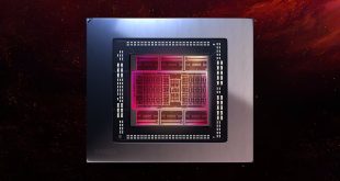
Taiwan Semiconductor Manufacturing Co. has successfully produced the first samples of Nvidia Corp.’s code-named GP100 graphics processing unit. Nvidia has already started to test the chip internally and should be on-track to release the GPU commercially in mid-2016.
3DCenter reports that Nvidia has sent the first graphics cards based on the GP100 graphics processor to its subsidiary in India, where it has a lot of hardware and software developers. No actual details about the chip or graphics cards on its base are known, but it is about time for the graphics giant to start testing its GP100.
Nvidia taped out the GP100 in June, 2015. Production cycle of TSMC’s 16nm FinFET process technology is about 90 days, therefore Nvidia got its GP100 from TSMC very recently. Right now the company is testing the chip and its drivers internally.
Nvidia’s GP100 graphics processing unit is based on the “Pascal” architecture and is made using 16nm FinFET+ process technology. The chip is expected to integrate up to 6000 stream processors and contain around 17 billion transistors. Graphics cards featuring the GP100 will carry up to 32GB of HBM2 memory.
Nvidia did not comment on the news-story.
Discuss on our Facebook page, HERE.
KitGuru Says: It is about time for Nvidia to start testing its GP100 now. What remains to be seen is when exactly the company plans to formally introduce its next-generation GPUs. If the first revision of the chip is fully functional, the company may move in introduction of the GP100 to the first quarter of the year.
 KitGuru KitGuru.net – Tech News | Hardware News | Hardware Reviews | IOS | Mobile | Gaming | Graphics Cards


Only to be sold for 900$ “JUST” because it is faster than the previous
Allow me to show you a@ fantastic ways to earn a lot of extra money by finishing basic tasks from your house for few short hours a day — See more info by visiting >MY___{DISQUS}___ID::
internal testing = multiplayer gaming 16 hours / day 🙂
It won’t be that crazy expensive but what the hell do you expect. New and better things are more expensive than old and shitty things, especially considering Pascal is a huge performance boost. Stick to the #60’s if you can’t afford it
jesus already testing the Chip.. were looking at A February release… Maybe march
Better than a 650$ AMD card that can be beaten by older 350$ AMD cards not using HBM
it will allow for up to 32 GB but will only carry maybe 4-8 max. even then because AMD has first rights to HBM2 and subsequent Memories sequels, they might not even get that high.
so if it goes the way you marked it out it’s going, within 10 years we will be paying around $2000 for a normal High end Card “just because it and it’s predecessors were*faster and better* building up the price for no real reason since every successor costs about 5 times less to make”
I tell u they gonna just test it out with HBM2 not use it in final builds. They will probably make their own stacked Vram
Wrong, wrong, mega wrong.
Skylake is a huge performance boost over a pentium D, does that make it more expensive? No.
Moores law applies to gpus as well.
it will be great but they dont have working memory controler ,,,,,
R&D is not free. I don’t know how you calculate that every successor costs 5 times less to make.
AMD have no “rights” over HBM because they are not manufacturing HBM.
The flagship maybe but the more mainstream will be priced competetivly (bad english)
Playing Bf maxed out 4k 300fps so they have to gimp the cards
I hope its minimum 6-8GB
no but they co created the technology, and under that, they get first rights to the chips from the manufacturers.
Wow Nvidia is trying to justify their use of HBM with some very powerful chip. I should say that thing is likely to rock 4K@60 and 1440p@120 without a problem…though Witcher 3 will be a little challenging. 😀
The Titan series will be 12GB.
… Maybe April …