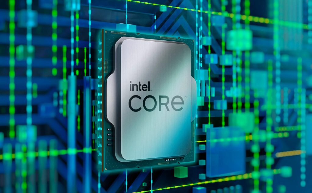
As technology advances, the demand for faster computation is increasing, leading chip designers to seek ways to integrate more components into processors. At IEDM 2023, during a technical session, Intel researchers demonstrated their latest technological breakthrough that will allow just that: 3D-stacked CMOS transistors with backside power and direct backside contact.
Intel claims this breakthrough will allow Moore's Law to continue scaling to higher performance in future semiconductors. Intel aims to have five chip nodes in four years and requires new chip designs to transition to the Angstrom Era. By then, specific physical properties within chips can no longer be precisely quantified in nanometers, forcing us to measure in angstroms (one ten-billionth of a meter).
During the technical session, Intel specialists demonstrated the 3D-stacked CMOS (complementary metal oxide semiconductor) transistors with backside power and backside contact. This results in complementary field-effect transistors stacked vertically at a scaled gate pitch of 60nm, allowing for more area efficiency (similar to how a multi-story building optimises area usage versus a single-story building). Backside power and direct backside connections mean that the processor's power-delivery interconnects are relocated under the silicon to make room for data interconnects above the silicon. Power interconnects can also be made bigger and, therefore, less resistive.
Intel's first implementation of backside power delivery, PowerVia, is expected to go into production in 2024. Researchers are also investigating other alternatives besides PowerVia.
Discuss on our Facebook page, HERE.
KitGuru says: Do you think this technology alone will keep Moore's Law relevant?
 KitGuru KitGuru.net – Tech News | Hardware News | Hardware Reviews | IOS | Mobile | Gaming | Graphics Cards


