Samsung and SK Hynix have much to show at the IEEE Solid State Circuit Conference (SSCC). The event, which is scheduled to run from February 18th to the 22nd in San Francisco, will see both companies showing their upcoming memory products, including GDDR7 memory, 16-layer HBM3E stacks, faster LPDDR5T and DDR5 memory, and 280-layer 3D QLC NAND flash.
According to @harukaze5719, Samsung will showcase GDDR7 memory chips at the event, providing updates over what was previously shown by Samsung in 2022. GDDR7 memory is primarily designed for gaming consoles and graphics cards, offering a massive bandwidth increase compared to GDDR6 and GDDR6X. Samsung is likely to introduce a GDDR7 chip that can handle 37 Gbps data throughput and has a density of 16 Gbit (2GB). The high speeds of GDDR7 memory technology are achieved thanks to the use of PAM3 signalling and the four read clock modes that help with power management when the device is not in use. Both NVIDIA and AMD are expected to use GDDR7 in their next-gen GPUs.

In addition to the 37 Gbps GDDR7 memory, Samsung plans to showcase other memory advancements at the 2024 IEEE-SSCC. The company is introducing a new 280-layer 3D QLC NAND flash memory with a density of 1 Tb, which will power the next generation of popular SSDs and smartphone storage. This chip has an area density of 28.5 Gb/mm² and a speed of 3.2 GB/s. To put this into perspective, the fastest 3D NAND flash types that power the current flagship NVMe SSDs use 2.4 GB/s chips.
Samsung is also introducing a new generation DDR5 memory chip with transfer speeds of DDR5-8000 and a density of 32 Gbit (4GB). This device has a symmetric-mosaic DRAM cell design and is based on Samsung's 5th generation 10nm class foundry node, optimised for DRAM products. This chip is remarkable because it enables PC memory manufacturers to produce 32GB and 48GB DIMMs in single-rank configuration with DDR5-8000 speeds, as well as 64GB and 96GB DIMMs in dual-rank configuration.
However, Samsung is not the only Korean memory giant to showcase its latest technology at the next IEEE SSCC. SK Hynix will also be there, demonstrating rival technology across both volatile and non-volatile memory segments. SK Hynix will be the second manufacturer to demonstrate GDDR7 memory after Samsung. The SK Hynix memory has a 16 Gbit density and can handle 35.4 Gbps, which is slightly slower than Samsung's 37 Gbps. SK Hynix, like Samsung, uses PAM3 I/O signalling and a proprietary low-power architecture.
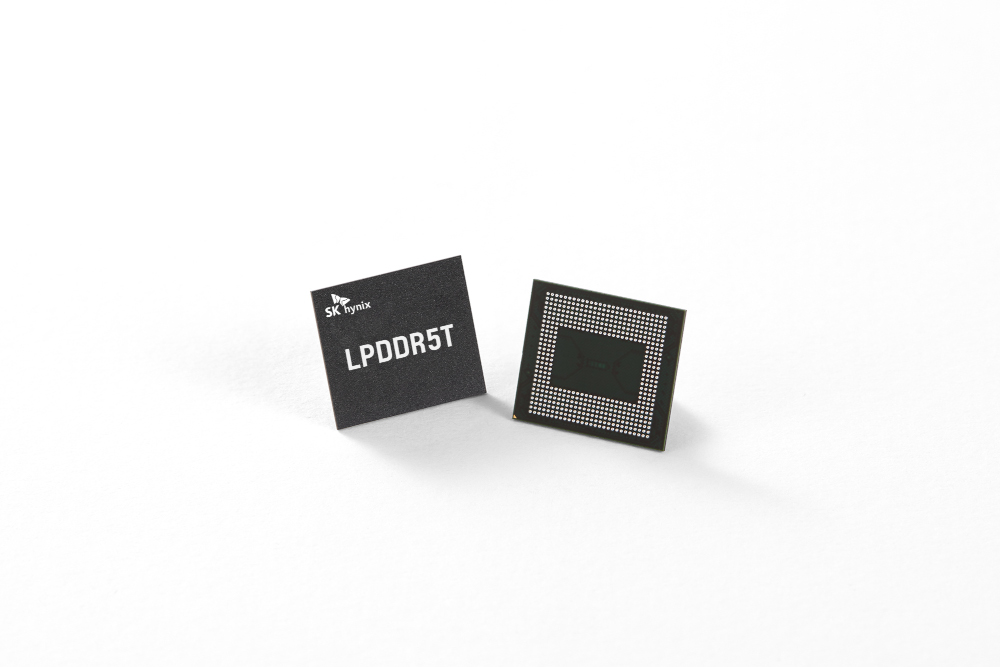
SK Hynix also has a new HBM3E product to show, a new 16-high 48GB (384 Gbit) HBM3E stack architecture that can handle 1280GB/s over a single stack. The stack employs an all-around power TSV (through silicon via) architecture and a 6-phase RDQS (read data queue strobe) method to optimise TSV space. Lastly, SK Hynix sessions will include the first demonstrations of their ambitious LPDDR5T (LPDDR5 Turbo) memory aimed at smartphones, tablets, and thin-and-light laptops. This memory delivers a data throughput of 10.5 Gb/s per pin and a DRAM voltage of 1.05 V. Such high data rates are possible due to the WCK-correction strategy employed, as well as the patented parasitic capacitance reduction technique and a voltage-offset calibrated receiver.
Discuss on our Facebook page, HERE.
KitGuru says: Of all the memory advancements to be showcased, which one is the most promising to you?
 KitGuru KitGuru.net – Tech News | Hardware News | Hardware Reviews | IOS | Mobile | Gaming | Graphics Cards


