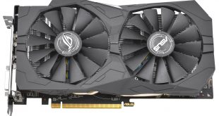
AMD is looking to keep the ball rolling with new GPU releases until the new Vega architecture arrives later this year. One of the methods AMD is doing this by is refreshing its existing GPU range to stay competitive, both the RX 470 and RX 480 are being refreshed to produce the RX 570 and RX 580.
This refresh is nothing AMD hasn't tried before, it executed a similar strategy when it refreshed the R9 290 and 290X GPUs in 2015 to release the R9 390 and 390X. RX 570, the focus of this review, is based upon the RX 470 from the current RX 400 series. At a fundamental level this is still the same graphics processing unit as before, 14nm and based on the Polaris architecture, but with a few tweaks to improve the end product.
These tweaks concern two key areas, standard clock speeds and power consumption. In terms of clock speeds the default clock speed for the RX 570 is now higher with a peak clock speed of 1244MHz compared to 1206MHz and a considerably higher base clock, 1168MHz versus 926MHz. The end result is that on average a stock RX 570 will always be operating at a higher frequency than an equivalent RX 470, though this comes at the expense of an increased TDP which rises from 120- to 150-watts.
The default memory frequency is also now higher, to the tune of 100 MHz actual, 400MHz effective, but the standard memory configuration of 4GB of memory remains unchanged. AMD may still allow board partners to offer 8GB versions of the RX 570, like it did with the RX 470, but for the capability of the RX 570 GPU anything above 4GB is likely excessive.
The second area of change, power consumption, is where AMD has altered power management techniques to increase power efficiency under a number of scenarios including multi-monitor, multimedia playback and system idle.
AMD has been able to achieve this by adding a third intermediate memory state to reduce power consumption, which sits alongside two existing memory states. To over-simplify, the current Polaris GPU effectively has two memory states, low and high, and most GPU activities (including having a second display) alter the memory state from low to high, increasing power consumption in the process. The new third intermediate memory stage now means the refined Polaris GPU has low, medium and high. In many cases a load activity can increase it to medium, before high, thus resulting in lower overall power draw.
AMD is using the RX 500 series launch as a platform to introduce a new feature it's calling Radeon Chill, which effectively reduces the frame-rate when the user is in-game but idle or AFK (away from keyboard) and then increases the frame-rate again when the user becomes active. It also caps “excessively high” frame rates to further reduce power consumption, though how this will be implemented is not clearly specified.
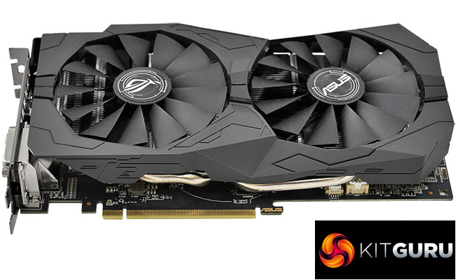
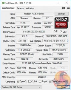
Our RX 570 review sample for today is the ASUS RX 570 Strix Gaming OC 4GB graphics card. This is factory overclocked 56MHz above AMD's stock settings for the RX 570 GPU while the GDDR5 memory remains unchanged at 1750 (7000) MHz. At a specification level the ASUS RX 570 Strix Gaming OC 4GB is virtually identical to the ASUS RX 470 Strix Gaming OC 4GB (see our review of that here) except with an extra 50MHz on the core clock and 100 (400) MHz on the memory.
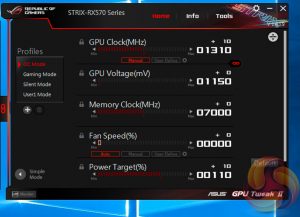
Like its RX 470 predecessor the ASUS RX 570 can toggle an OC Mode if the user installs the ASUS GPU Tweak software. In the case of the RX 470 it bumped the core clock from 1250 to 1270MHz, with the RX 570 it increases it from 1300 to 1310MHz and increases the power target from 100 to 110%. A minor change but an easy one for buyers who lack the confidence to overclock themselves.
| GPU | AMD RX 480 | AMD RX 580 | AMD RX 470 | AMD RX 570 | AMD R9 390 |
Nvidia GTX 1050 Ti | Nvidia GTX 1060 |
| Streaming Multiprocessors / Compute Units |
36 | 36 | 32 | 32 | 40 | 6 | 10 |
| GPU Cores | 2304 | 2304 | 2048 | 2048 | 2560 | 768 | 1280 |
| Texture Units | 144 | 144 | 128 | 128 | 160 | 48 | 80 |
| ROPs | 32 | 32 | 32 | 32 | 64 | 32 | 48 |
| Base Clock | 1120 MHz | 1257 MHz | 926 MHz | 1168 MHz | Up to 1000MHz | 1290 MHz | 1506 MHz |
| GPU Boost Clock | 1266 MHz | 1340 MHz | 1206 MHz | 1244 MHz | Up to 1000MHz | 1392 MHz | 1708 MHz |
| Total Video memory | 4096 or 8192 MB | 4096 or 8192 MB | 4096 or 8192 MB | 4096 MB | 8192 MB | 4096 MB | 6144 MB |
| Memory Clock (Effective) |
1750 (7000) or 2000 (8000) MHz | 2000 (8000) MHz | 1650 (6600) MHz | 1750 (7000) MHz | 1500 (6000) MHz | 1752 (7008) MHz | 2002 (8008) MHz |
| Memory Bandwidth | 224 or 256 GB/s | 256 GB/s | 211 GB/s | 224 GB/s | 384 GB/s | 112 GB/s | 192 GB/s |
| Bus Width | 256-bit | 256-bit | 256-bit | 256-bit | 512-bit | 128-bit | 192-bit |
| Manufacturing Process | 14nm | 14nm | 14nm | 14nm | 28nm | 16nm | 16nm |
| TDP | 150 W | 185 W | 120 W | 150 W | 275 W | 75W | 120 W |
 KitGuru KitGuru.net – Tech News | Hardware News | Hardware Reviews | IOS | Mobile | Gaming | Graphics Cards


Well AMD… https://uploads.disquscdn.com/images/391b049c1e1753b69970b6cfd66cd81ceb1593cec805f6fb20b18af365a9b680.jpg
Hey Ryan, mind sharing the bios for this card? Can be dumped/submitted using gpu-z. Thanks