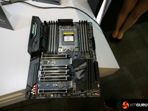
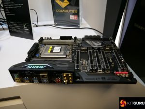
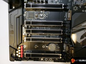
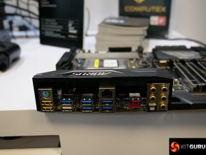
A few weeks back, AMD officially announced that it would be launching its new HEDT platform this summer, with the 16C/32T ‘Threadripper' CPU set to be the star of the show. As you would expect, this means motherboard makers are now beginning to give us a look at their plans for AMD's X399 chipset, with Gigabyte bringing its first X399 Aorus Gaming 7 motherboard to Computex this week.
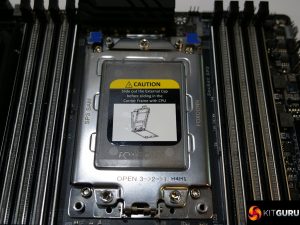
While much of the details surrounding X399 are still under NDA, we are able to show you some images of the motherboard, though the socket has been kept hidden from view. For X399, AMD's socket is officially named TP4.
From what we have heard, AMD's TP4 socket is more expensive to make than Intel's equivalent. However, the cost of AMD X399 motherboards are expected to sit in a similar price range to X99/X299.
Aside from that, this Gigabyte Aorus Gaming 7 motherboard will retain many of the same features found on the X299 Aorus Gaming 7 board. However, AMD's version will lack Intel LAN ports, optane memory support etc.
KitGuru Says: There has been a lot of discussion surrounding Intel's new Core-X CPUs and X299 today, so it's nice to see some AMD news ahead of the company's own conference tomorrow. Still, with AMD's chipset being called X399, I do wonder what Intel is going to do when it introduces its next HEDT chipset.
Credit to Leo Waldock for additional reporting and detail.
 KitGuru KitGuru.net – Tech News | Hardware News | Hardware Reviews | IOS | Mobile | Gaming | Graphics Cards



AMD is totally trolling Intel with these name choices….. R3, R5, R7, B350, X370, and now X399
Edit: Really intel should have been forward thinking and trademarked all the future name iterations they were planning to use…. unless they are not planning to use that and instead will switch to a different naming scheme. We shall see….
the TP4 looks like an lga mechanism?
They tried trademarking the 486SX & 486DX processors back in the 90s but lost due to the fact you can’t trademark a number or letter. That’s why they named the 586 processor the Pentium.
Ah I do remember reading about that. Good point.
It is, Threadripper uses a LGA package vs the Ryzen “Summit Ridge” AM4 socket which is PGA. You probably already knew that though. 🙂
Intel can still use the X399 moniker for there next iteration of the HEDT platform. Just because AMD is using it now, means nothing.
Interesting to see this go LGA rather than their familiar PGA arrangement. I wonder as to the reasoning for doing so? Were the chips just not going to work any other way from a manufacturing/fab point or was it something else?
They are using the same socket as their server platform which they are using lga for. Pga is only for consumer chips.
But this is being marketed… at consumers. So, to that end, this doesn’t make all that much sense. If they went LGA for the EYPC CPUs since those are obviously purpose designed and built for server applications, that would be something entirely different.
LGA has a greater connection density. PGA has pins on the Chip which are a fulcrum (a lever to bend and apply a very tiny amount of unwanted pressure).
If a pin breaks on either then it’s practically ruined (not impossible to repair if you’re desperate).
Cheap Chips and expensive MB, use PGA.
Expensive Chips and cheap MB, use LGA; even more so when there’s a lot of pins.
PGA is (usually) gold pins which must be kept straight and forced into a hole.
LGA is (usually) bent pins that touch a pad on the Chip (like PGA with all the pins cut off, leaving the circular pads). The pad on LGA can be a small oval (instead of the larger circular area of PGA) and the springing action of the LGA’s bent pins act on the (potentially) lower pressure socket holder.
LGA takes a bit less gold, certainly far less on the Chip, reducing the Chip cost and probably using less gold on the MB’s pins since only the tip needs to be plated.
The Chip is created first (ala which came first, the chicken or the egg) and LGA makes the Chip cheaper and more reliable. After the Chip is made then MB Mfgs can choose to make a MB for the Chip – MB’s are not made first and then the CPU must conform, so it’s the Dog that wags the tail (the expensive and more technical device decides what goes where).
If we were to never upgrade the whole thing could be Wave Soldered. LGA could be Wave Soldered and PGA can not – so LGA does double duty (that is not popular enough to be utilized very often with CPUs).
Did I miss something?
Thanks for the (unnecessary) lesson covering the differences between the two. I understand the two applications just fine; my wonder has to to with AMD’s rationale to switch it. That’s all.
prolly too big for a pga
If that is so, then the move to LGA makes sense.
HEDT != Consumer
You know what that acronym means, right? High End Desk Top. So, how is that not marketed at consumers?
HEDT, which means Enterprise and high end workstations
These aren’t something you’d buy for your home computer. Most sales will be b2b
We’ll see.
You can drive a Bugatti in snow, that doesn’t make it normal
There is no “we’ll see”
Statistical outliers don’t count
Actually the platform (Epyc) was designed for professional and businesses. they just decided to use the same platform for the consumer HEDT market (renamed to threadripper with some tweaks) to save money, just like Intel did.