

AMD's Ryzen CPUs have been a huge success throughout 2017 but it is time to start looking towards the company's plans for next year. AMD has said in the past that we will see a Zen 1 refresh before the jump to Zen 2 architecture, and now it looks like we know when to expect that to happen.
As part of a recent presentation, AMD began showing its lineup of Ryzen processors for 2018, which will kick off with Ryzen 2 in Q1. This means between January and March, we should see these processors launch. This is known as the ‘2000 series', with the Ryzen 7 1800X being bumped up to the Ryzen 7 2800X, the 1700X replacement will be the 2700X and so on.
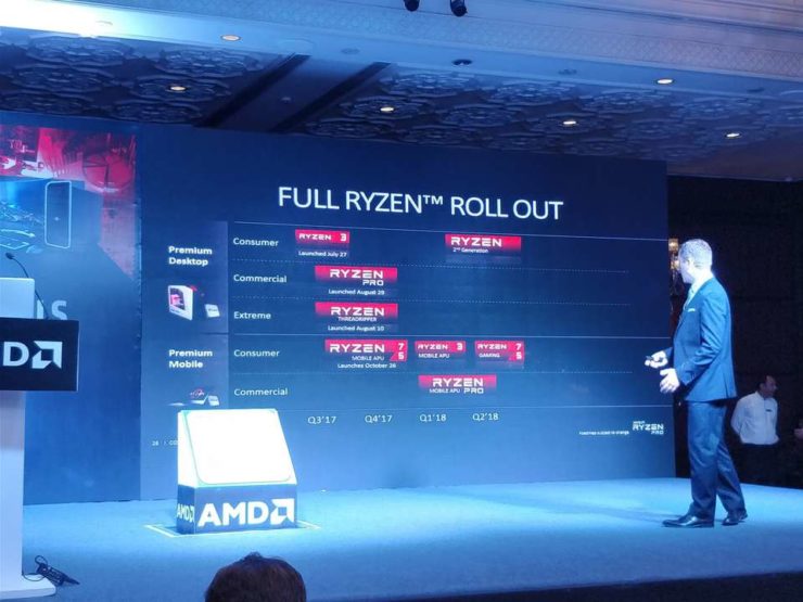
Presentation slide via moepc.net
According to the folks at wccftech, these processors will be based on the 12nm process node. We should apparently expect new Ryzen 7 chips in late February, followed by Ryzen 5 and Ryzen 3 in March. Those timings could of course change over the next couple of months. As for specific improvements we should expect, support for higher DDR4 RAM frequencies and slightly higher clock speeds are said to be on the way.
These new Ryzen Zen+ processors will be pitted against Intel's Coffee Lake chips. Intel is set to release new Coffee Lake SKUs in the first half of 2018, with rumors indicating that we will see Z390 motherboards brought to the table alongside a new 8C/16T Core-i7.
KitGuru Says: While the Q1 release date seems set in stone due to AMD's presentation slides, there is still a lot of rumor surrounding the specs of AMD's 2018 Zen refresh. We should learn more soon enough though, as CES is just around the corner.
So the Ryzen refresh would they more likely to be considered Ryzen 1.5 refresh on 12nm & not actually the Ryzen 2 Zen 2 CPU’s? I am going to assume the Zen 2’s will be labeled as the 3000 series then.
Intel is MIA on 10nm. 10nm may never happen (for Intel CPUs).
Current Lithography is at its limits until EUV proves viable.
AMD will continue to ramp and gain share on Intel, especially now that full Ryzen lineup including mobile, plus EPYC servers for Cloud will really begin in 2018, as Lisa Su has said.
Samsung is adopting EUV quicker than its competitors, giving its foundries a head-start as they transition past 7nm. https://cdn57.androidauthority.net/wp-content/uploads/2017/11/Samsung-4nm-RoadMap.jpg
zen 2s will most likely be on 7nm since in mid to late 2018 global founderies is going to do a limited run on 7nm.
As far as we know… Ryzen refresh (or Ryzen+) will be made on 12nm LP and released February 2018.
Late 2018 is slated for 7nm and Ryzen 2 (and probably Navi).
It would also appear that sometime in 2019, Ryzen 3 is slated to be released as well on 7nm.
Any idea what they will go to from there?
From what I know thus far, the upcoming 12nm LP and 7nm are IBM based processes designed for high performing parts.
AMD also previously released some slides indicating Ryzen 3 on 7nm as well in 2019/2020… but nothing on a smaller process.
Ryzen is based on Zen 14nm. Ryzen’s next release (you call it a refresh, but its not, it is a full process upgrade from 14nm to 12nm) has been officially named Ryzen 2 and will be on 12nm. Ryzen 3 will be based on 7nm Zen 2 architecture, and will “probably” be the 3000 series, as I suspect you have guessed correctly given the nature of the AM4 socket accepting it. Newer architectures can receive version numbers such as 1.1 or 1.5 (if you like), but actual new “released” products are 1st, 2nd, 3rd, 4th and 5th etc (there is no such thing as one and a half retail product unless you take a chain saw to it). So the “next” a.k.a 2nd Ryzen release in early 2018 is obviously Ryzen 2, as that is the only thing that makes any sense. 3rd release of Ryzen will therefor be Ryzen 3.
It seems if you read between the lines of what Intel have stated 10 nm will be for Cannon Lake, but that will be the small Atom based Celerons and Pentiums and not the Core line, just like Gemini Lake. The Core line will seemingly have to wait until 10 nm + or 10 nm ++. This is due to their 10 nm apparently not being as good performance wise as 14 nm ++, which is what Kaby Lake and Coffee Lake use. Either 10 nm + or 10 nm ++ should apparently catch up though.
Global Foundries are also working on EUV, but they are likely licencing an EUV based node off Samsung just like they licenced 14 nm and 10 nm off Samsung.
7nm is produced by GlobalFoundries in house, and I haven’t read anything on 10nm licensing from Samsung. I do know about 14nm LPP licensing from Samsung , because GlobalFoundries failed to produce it’s own 14nm(20nm).
https://en.wikichip.org/w/images/f/fb/intels_10%2B_and_10%2B%2B.png
10+ may allow for higher frequency
https://i.imgur.com/VhlCFwb.png
https://en.wikichip.org/wiki/intel/microarchitectures/ice_lake#All_Ice_Lake_Chips
The slide was a fake, those numbers aren’t real.
Yep you are totally right. It is good to see AMD has straight up releases for the Ryzen’s and all coming at the long wait we had with their older FX CPU’s. If they follow through with their release dates it will keep a fair amount of pressure on Intel which is good for us the consumers as it may get us lower prices and faster tech a lot sooner.
The difference in 14nm and 12nm is the change in transistor libraries from 9T to 7.5T. This is what provided the 15% increase in transistor density, and 10% increase in transistor performance.
However, we need to keep in mind that 10% increase in transistor performance is when coming from TSMC’s 16nm high performance process.
The 14nm Glofo process is suited for low performance and low power… that’s why Ryzen and Vega have issues achieving high clocks. Ryzen is capped at roughly 4GhZ due to this, and Vega can’t go above 1450MhZ (roughly) without suffering from large power draw.
The transition to 12nm LP should eliminate the 4GHz barrier for Ryzen and allow Vega to be clocked much higher on both core and HBM without having high power draw (though AMD should try to not overdo the voltages on Vega – but this may be an issue since they do this historically to improve yields).
~4GHz base clock ~4.4GHz XFR, and “hopefully” some low hanging fruit in the IPC department(5%) would be nice!
https://www.extremetech.com/wp-content/uploads/2017/09/AMD-12nm.png
We’ll see… but I’m expecting about Intel level clocks on the baseline for Ryzen refresh, if not better (at the very least the 6 cores/12 threads and 8 cores/16 threads should be able to match Intel in baseline single-threaded and multi-threaded clocks).
Ant any rate, Ryzen+ should be able to close the gap with Intel in clock rates (as AMD wants to keep same TDP) thanks to the new process.
Bear in mind that Intel is using a 14nm process suited for high clock speeds.
I think 12nm LP is based on IBM’s upcoming 7nm high performing process (which will allow 5GhZ baseline)… as both have LP (leading process) designation.
As for IPC improvements… not sure about that for a refresh… but again, bear in mind that most applications and software is optimised for Intel or uses Intel compilers (which could explain why Intel has a 5% higher IPC).
Overclocked Ryzen with optimisations was actually able to keep up with overclocked i7’s… and since Intel’s overclocked higher, it was actually quite a bad blow for Intel.
That’s why Intel created 500 MhZ – 1000 MhZ higher clocked CPU’s to give an impression of being better.
Most people don’t understand how limited AMD is by using Glofo process (present company excluded).
AMD is still building on the same 14nm process, but changing the transistor libraries from 9T to 7.5T. It’s going to be basically the same design with transistors capable of “slightly” higher clocks. 4.4GHz with XFR is being realistic. The 7nm will be based on 6T libraries and GlobalFoundries own 14nm process/IBM not Samsung. It’s possible to see 5GHz+ ranges from the 7nm, but not from the 12nm.
http://btbmarketing.com/iedm/
[spoiler][img]http://btbmarketing.com/iedm/docs/29-5%20Narasimha_Fig%202.jpg[/img]
[img]http://btbmarketing.com/iedm/docs/29-5%20Narasimha_Fig%2011.jpg[/img]
[img]http://btbmarketing.com/iedm/docs/29-5%20Narasimha_Fig%2014.jpg[/img]
[img]http://btbmarketing.com/iedm/docs/29-5%20Narasimha_Fig%2016.jpg[/img][/spoiler]
[quote]
Globalfoundries researchers will present a fully integrated 7nm CMOS platform that provides significant density scaling and performance improvements over 14nm. It features a 3rd-generation FinFET architecture with self-aligned quadruple patterning (SAQP) used for fin formation, and self-aligned double patterning for metallization. The 7nm platform features an improvement of 2.8x in routed logic density, along with impressive performance/power responses versus 14nm: a >40% performance increase at a fixed power, or alternatively a power reduction of >55% at a fixed frequency. The researchers demonstrated the platform by using it to build an incredibly small 0.0269µm2 SRAM cell. Multiple Cu/low-k BEOL stacks are possible for a range of system-on-chip (SoC) applications, and a unique multi-workfunction process makes possible a range of threshold voltages for diverse applications. A complete set of foundation and complex IP (intellectual property) is available in this advanced CMOS platform for both high-performance computing and mobile applications.
Graph (a) above shows the improved power and performance responses of the new platform compared to the previous 14nm node; (b) shows that the 7nm SRAM cell demonstrated ~2x speed enhancement and >2x density scaling improvement vs. 14nm; (c) shows an example of two BEOL stacks, with the cross-section focused on the 1X and 2X levels; and (d) shows an improved electromigration lifetime compared to the prior node.
(Paper 29.5, “A 7nm CMOS Technology Platform for Mobile and High-Performance Compute Applications,” S. Narasimha et al, Globalfoundries)[/quote]
Anyone have info on HEVC (H.265) encoding/decoding on Ryzen or Threadripper???
The slightly higher clocks is not something I agree with.
I think we will be seeing around 4GhZ and 4.4GhZ baseline on 12nm with turbo boost to 4.6 GhZ or 4.8 GhZ across all cores (with an overclock possibly allowing 5 GhZ).
The architecture and design might be the same, but even AMD will need to make adjustments to accommodate 15% higher chip density for Ryzen refresh.
Plus, the 12nmLP is designed for high power and high performing parts… this won’t be a small clock increase… it will likely be in the range of 20%- 30%.
Basically, we’re looking at increases of about 500MhZ to 1GhZ on Ryzen at baseline.
How well it overclocks (if it does) depends on the process – but my point is that Intel won’t have a clock advantage anymore most likely.
And Intel’s 5 GhZ boost comes on 1 core… not across all cores… plus, some motherboard manufacturers come with a ‘feature’ that overclocks Intel CPU’s right out the door (which also makes them run hot and unstable).
TSMC’s 16nm allows for high clocks on Pascal for instance (and it enjoyed about 30% uplift over Maxwell).
Transitioning to 12nm LP will give Pascal 10% bump up in performance from clocks alone and a decrease in power consumption.
AMD’s Vega for instance will basically see what Pascal saw going from Maxwell (radical clock bumps for same power draw) and an extra 10% boost in performance and further efficiency gains from process improvements (lower voltages, etc.).
Ryzen will likely experience the same 20%-30% increase in clocks most likely at same power draw.
I could easily be wrong of course… I’m just extrapolating based on what the GPU’s were able to achieve when transitioning – and while I know it’s not directly comparable/applicable to a CPU, that’s why I said 20%- 30% increase in clocks on Ryzen from process improvements (while keeping in the same TDP).
Looking at the graph I link comparing 14nm to 7nm transistor performance and power consumption. We can make some estimations on base clock and XFR clock frequencies.
14nm 1.3 Normalized Frequency 7nm Soc 1.7 Normalized Frequency
1.3 to 1.7 is 30.7%@less power consumption
30.7% X 3.6GHz = 4.7052GHz
30.7% X 4.1GHz = 5.3587GHz
7nmHPC
1.7 to 2.1 is 23.5% @~2.5x power consumption
23.5% X 4.7052 = 5.810922GHz
23.5% X 5.3597GHz = 6.6179945GHz
12nm is 14nm with 7.5T libraries, and 7nm has 6T libraries. It’s hard to imagine 12nm much further beyond an XFR of 4.5GHz.
http://btbmarketing.com/iedm/docs/29-5%20Narasimha_Fig%202.jpg
It’s not hard to imagine going to 4.5 GhZ or slightly over that when you have existing TDP’s of 65W to 95W to fill and 15% higher chip density on a process designed for high clocks and high power (especially when you are coming from a process node designed for low power and low clocks).
Node shrinks aren’t be all and end all.
It depends on WHAT kind of process it is.
We’re talking about a 10% performance uplift on 12nmLP coming from 16nm which is already designed for high clocks and high powered components.
Since AMD is coming from a 14nm process designed for low clocks and low power (mobile parts essentially), you are bound to experience higher gains and.
That’s why Intel’s 14nm and AMD’s 14nm aren’t the same.
They are comparable in sizes perhaps but, Intel’s allows high clocks… AMD’s does NOT.
This is a very important distinction to note.
But I digress, we need to wait and see.
In the meantime, it might be noteworthy to read this:
https://forextv.com/top-news/globalfoundries-introduces-new-12nm-finfet-technology-for-high-performance-applications/
You are correct them not being the same design. 14nm/12nm is made for 3.5GHz operations. Changing from 9T to 7.5T transistor libraries will increase the performance, but not nearly as much as 5GHz(you are reaching beyond the limits of the design). 7nm LP is rated for 5GHz operations. Right now it take imagination to make 5GHz happen for the 3.5GHz design.
https://www.globalfoundries.com/sites/default/files/product-briefs/7lp-product-brief.pdf
Also, you can find the same information for other products and news on globalfoundries website.
https://www.globalfoundries.com/news-events/press-releases/gf-press-releases
Actually it’s the 14nm from glofo that’s made for 3.5 GhZ operations.
12nmLP is designed for high performance or its own datasheet.
Apples and oranges.
14nm from Glofo and upcoming 12nm LP are NOT the same process… that’s why you can’t compare performance gains coming from a low power process to a high powered one.
12nmLP is just zen 14nmLLP with 7.5T libraries relabled 12nmLP. It’s the same design, we “hope” they increased IPC via “low hanging fruit”, but there is nothing published confirming this. It’s more Apples to Apples than you realize. They did redesign the process for 5GHz operations. Information released to date shows 14nmLPP designed for 3GHz operations, relabeled 12nmLP using 7.5T libraries.
“It’s not a full redesign, but there is some design work to move into it,” said GlobalFoundries Chief Technology Officer Gary Patton in a press briefing.
https://www.hpcwire.com/2017/09/24/globalfoundries-puts-wind-amds-sails-12nm-finfet/
“GlobalFoundries said the new 12nm platform, on track for risk production in the first half of 2018, will offer a 15 percent improvement in circuit density and a greater than 10 percent performance boost over industry 16nm FinFET solutions. (There’s an intended improvement over 14nm too, of course, but no specific figures were offered.) Manufactured at the GlobalFoundries’ Fab 8 factory in Malta, NY, 12LP (LP stands for Leading Performance) builds on GloFo’s 14nm FinFET platform in high-volume production since early 2016.
“It pushes new design rules and some new constructs,” said GlobalFoundries CEO Sanjay Jha, “but our fundamental focus is to enable people who have already designed 14nm to be able to migrate to 12LP. It is a cost reduction path as well as a performance enhancement path for a number of our customers, including AMD.”
The 12nm technology is an intermediate step on the way to the 7nm FinFET node, slated for risk production in the first half of 2018. “It’s not a full redesign, but there is some design work to move into it,” said GlobalFoundries Chief Technology Officer Gary Patton in a press briefing. “We want it to be as close to an extension of 14 as possible. If you’ve invested all this design IP in 14, you want to extend that as much as possible.
https://6lli539m39y3hpkelqsm3c2fg-wpengine.netdna-ssl.com/wp-content/uploads/2017/09/GTC2017-12LP-12nm-FinFET-768×709.png
Read the second bullet point in the picture”minimizing design rework” is also clue.
I meant 7 nm not 10. I read somewhere (I forgot where) that GF said that 14 nm is not the only node they licenced from Samsung. Since Samsung does not have a 12 nm node and GF is skipping Samsung’s 10 nm node that leaves only 7 nm. Unless maybe they originally had plan to use Samsung’s 10 nm node and cancelled those plans.
But given how unreliable GF are at making their own nodes (they had huge delays on 1 or two nodes before 14 nm as well) I hope you are wrong about them making their own 7 nm node.
Maxwell to Pascal was from 28 nm to 14 nm, i.e., an improvement of two whole nodes at once. Even with the switch from LPP to LP, Ryzen to Ryzen+ is 14 to 12nm, which is only a half node so likely that it cannot match the improvements that come from 2 node improvements at once.
GlobalFoundries in the past has been riddled with problems and delays. My hope is that with the inclusion of IBM assets and personnel the future will be different going forward. GlobalFoundries has been working on their own 7nm design capable if 5GHz operations. Samsung has to make 7nm before they can license it out, and it will be for Samsung smart phones using low power and low fequency. https://www.globalfoundries.com/sites/default/files/product-briefs/7lp-product-brief.pdf
Patton: We are doing it completely on our own.
SE: Is GlobalFoundries co-developing 7nm technology with Samsung?
Patton: We are doing it completely on our own. We had the collaboration on 14nm. We still partner with them on what I’d call pathfinding in Albany. As part of the deal with IBM, Albany used to be an all-joint-development alliance. Then it was spilt into two parts. Half of the facility continues to do the joint development work, which IBM leads. Think of that as pathfinding for 5nm and beyond. And the other half is a proprietary IBM-GlobalFoundries corridor, which is specifically focused on accelerating things into Malta. Those could be performance elements for 7nm and 7nm plus. In fact, I would envision we’ll have a bunch of performance kickers at 7nm. This will be a long node.
https://semiengineering.com/inside-fd-soi-scaling/
But you are forgetting that 14nm node on which Vega was made is designed for low power and low clocks.
12nmLP is designed for high clocks (LP stands for ‘leading performance’ … not ‘low power’).
There are bound to be bigger differences on how a transition to 12nm LP will affect Vega vs Pascal.
Pascal is already coming from a process designed for high clocks so its bound to see lesser gains than Vega (which was limited by the low power manuf. process).
I’ve read it… and I also read the fact that this 12nm LP process is designed for high performance desktop parts (aka high clocks).
14nm LPP on which original Vega is built on is NOT designed for high clocks.
That’s why the processes aren’t the same and why Vega will likely experience much higher than 10% performance boost.
Glofo 14nm is designed for low clocks and low power while 12nm LP is designed for high power and high clocks.
It’s the same as comparing Intel’s 14nm and Glofo 14nm… Intel’s is designed for high clocks (hence why Intel can clock higher than Ryzen), whereas Ryzen is limited to ~4GhZ.
And despite them wanting to minimising design work, the 12nmLP gives you 15% higher chip density, so adjustments will be required (however small they might end up).
Okay, I concede this conversation is not evolving. The great thing is that we will only have to wait 2 or 3 months to revisit this topic, which I’m sure you won’t forget what I’ve said here!
I agree the conversation is spinning in circles at this point and again that we don’t have long to wait to see the results of this process and Ryzen/Vega refreshes
I am not forgetting it at all. In fact this quote from my post makes it clear that I not only remembered it but took it into consideration: “Even with the switch from LPP to LP, Ryzen to Ryzen+ is 14 to 12nm,
which is only a half node so likely that it cannot match the
improvements that come from 2 node improvements at once.” (Emphasis added to highlight the part that makes it clear.)
My point was that even accounting for the switch from LPP to LP a half node improvement in highly unlikely to be able match a double node improvement. Especially when the half node is so small as to be a mere 2nm improvement. That would take significant architectural improvements as well, which will not be until Zen 2.
In fact, Pascal to Maxwell was more than just a 2 node improvement. It was also the switch to FinFET, which Intel and all Fabrication companies say is almost as good as an additional node improvement. So Maxwell to Pascal was the equivalent of a 3 node improvement. I don’t see the switch from LPP to LP and a mere 2 nm improvement equaling a two node improvement and a switch to FinFET.
I think Ryzen+ will likely be a lot better than some are expecting due to the switch from LPP to LP. In fact that will help more than the 2 nm improvement. But it likely won’t be as good as Maxwell to Pascal. Zen to Zen 2… maybe. But nor from Zen to Zen+. If it was that big an improvement I am highly doubtful that AMD would call it a mere refresh.
EDIT: BTW, I know what LPP and LP stand for and that the switch from LPP to LP is a big deal.
Then what happened to the second node they licenced off Samsung (whichever one it was)? Did they scrap those plans? That seems like an expensive (and thus risky) move if so. They had already licenced it so still have to pay for the licence even if they scraped the plans.
But this is bad news since they have not been reliable at making their own nodes for a long time. At best they have delivered them late and not attained good volume. They should have stuck with the licencing plan.
Hopefully you are right about the IBM thing and I am wrong about them going it alone being bad. Though if they are using IBM assets and personel then he was talking nonsense when saying, “We aew doing it completely on our own.” That is not doing it on their own at all.
It seems that changing their plans is something they have been doing a fair bit recently. In addition o the above, AMD previously listed Zen+ as 14 nm + but now they say it is 12 nm. This shows that GF changed their plans from doing 14 nm + to 12 nm. The question is, did they change the plans to suit AMD or did their change of plans necessitate AMD changing their plans?
Sadly, if leaks/rumours are to be believed the Vega refresh, Vega 20, is going to be for HPC/workstations only and not gaming cards. It also seems to double the RAM via doubling the number of HBM stacks and therefore memory bandwidth. Therefore we might not know how much of Vega 20’s improvements come from the switch to LP as it’d be hard if not impossible to single that part out from the overall performance gains.
EDIT: Separating said performance gains will be even harder if AMD manage to enable the missing Vega features on Vega 20 unlike on Vega 10. But hopefully they will figure out how to get those working on both.
There is also the question of whether or not the Zen/Zen+ architecture can even handle such high clocks as anywhere near the clocks you are talking about. Architectural designs matter too, not just whether or not an LP or LPP node is used. It might be able to handle such clocks, it might not. We simply don’t know yet. The same goes for Vega 20.
Perhaps you can provide a link to where they licensed another design from Samsung, because I’ve never heard any about it. 14nm is the only one they licensed. Here are the links: “The terms of the deal state that GF will continue manufacturing Power processors for IBM for at least the next ten years and that the manufacturing centers in East Fishkill will remain open and fully staffed.”
https://www.extremetech.com/computing/192430-ibm-dumps-chip-unit-pays-globalfoundries-1-5-billion-to-take-the-business-off-its-hands
Also, Santa Clara, Calif., July 1 2015: GLOBALFOUNDRIES today announced that it has completed its acquisition of IBM’s Microelectronics business.
“With the acquisition, GF gains differentiated technologies to enhance its product offerings in key growth markets, from mobility and Internet of Things (IoT) to Big Data and high-performance computing. The deal strengthens the company’s workforce, adding decades of experience and expertise in semiconductor development, device expertise, design, and manufacturing. And the addition of more than 16,000 patents and applications makes GF the holder of one of the largest semiconductor patent portfolios in the world.”
“Moreover, the transaction builds on significant investments in the burgeoning Northeast Technology Corridor, which includes GF’s leading-edge Fab 8 facility in Saratoga County, NY and joint R&D activities at SUNY Polytechnic Institute’s College of Nanoscale Science and Engineering in Albany, NY. The company’s presence in the northeast now exceeds 8,000 direct employees.
The acquisition includes an exclusive commitment to supply IBM with some of the world’s most advanced semiconductor processor solutions for the next 10 years. GF also gets direct access to IBM’s continued investment in world-class semiconductor research, solidifying its path to advanced process geometries at 10nm and beyond”
https://www.globalfoundries.com/news-events/press-releases/globalfoundries-completes-acquisition-of-ibm-microelectronics-business
Now, the 12nm is just a label it’s really closer to 14nm+, because they really only changed the transistor libraries from 9T to 7.5T, which will offer a slight performance boost 300-400MHz, and we “hope” they made some changes from picking up some “low hanging fruit” to increase IPC ~5%. I wouldn’t worry about GlobalFoundries too much, because acquisition of IBM Microelectronics Business gives me a lot more faith in their ability to perform.
I don’t remember where as it was a long time ago that I read/heard it. I think it was the 10 nm node as there was a time when GF talked about the 10 nm node before dumping those plans to do 12 nm and 10 nm instead. But now that I think about it some more I think the source said “will licence” not “have licenced”. So perhaps they were merely considering licencing 10 nm from Samsung as well as 14 nm. Also, perhaps the reason both plans were dropped was that they decided they’d rather do an LP node of their own rather than licene another LPP node.
So IBM is a major partner for GF now? That is good. Before that they relied too much on AMD as their only major partner for their own good.
GF getting access to IBM’s research is a great deal for everyone. IBM is a very capable company in that regard so anything they get from IBM will be quite capable and reliable. That should enable them to better compete with TSMC on power draw, performance, reliability and production levels as IBM is better on those fronts than GF has been. They and their customers will benefit a lot from that, but it is allso good for consumers that there will be extra competition against TSMC.
Well, as I understand it 14 nm + wasn’t necessarily even going to have the library change. It was simply going to improve node’s reliability and performance/power draw. Basically it was simply going to be an improvement of Samsung’s LPP node. So 12 nm still seems to be a bigger improvement than GF and AMD originally planned for. I just wonder if that was at AMD’s or GF’s behest.
TomsHardware has a comprehensive article on overclocking Ryzen past 5GhZ using liquid nitrogen and running benchmarks using those clocks:
http://www.tomshardware.co.uk/overclocking-amd-ryzen-ln2,review-33950.html
See the humongous voltages required to reach those clocks?
The architecture ain’t the issue here… it’s the manuf. process being pushed well past it’s breaking point because it simply wasn’t designed to run on those speeds.
As for the switch between the types of processes being used… I am not trying to glorify 12nmLP beyond its capabilities… I’m merely saying that AMD is likely going to see far better results with this new process for both Ryzen and Vega than say Nvidia would because AMD is juping from a low power process to a high powered one.
Nvidia is merely side-grading from one high performance process to another one (16nm to 12nmLP), so their Pascal refresh for example wouldn’t see big gains.
I am aware that Maxwell to Pascal jump was more in the node itself, but the architecture itself remained unchanged… Pascal is basically an overclocked Maxwell.
AMD has been stuck using low power process from Glofo for a long time now.
Clock per clock, both Polaris and Vega are faster than Nvidia.
Look at GTX 1060 and RX 580.
1060 has a 249 higher clocks than RX 580, and yet, 580 is either same in performance or better in DX12 and Vulkan.
Similar ratio applies to Vega.
Also, when undervolted, AMD GPU’s power consumption goes down to Pascal levels.
In mobile space, the RX 580 in Asus ROG GL702ZC laptop was restricted to 68W. The GTX 1060 is restricted to 80W.
Performance in actual games is again pretty much the same between the two GPU’s while the RX 580 outperforms 1060 in DX12 and Vulkan – but it’s now actually MORE efficient than 1060.
Also, that mobile RX 580 was underclocked by 20% from desktop (so, just below desktop 480 levels).
That’s why I’m saying that we can’t expect a mere 10% performance improvement only when you remove manuf. process as a limiting factor.
Now, AMD want’s to preserve 65 and 95W TDP’s for Ryzen refresh.
Transitioning to 12nmLP would allow for much higher clocks under the same TDP envelope… in the ballpark of around 20%… maybe 30% – depending on how good the process turns out to be – but I doubt we will only see 10% gains under same TDP.
AMD was able to ‘keep up’ surprisingly well with a manufacturing process that handicapped them from achieving efficient high clocks.
Yes, the power draw on Vega was not good in relation to Pascal, however, I do think Vega will no longer have an issue with clocks reaching Pascal levels and effectively surpass it in performance (considering that at LOWER clocks, Vega is basically matching or outperforming Pascal counterparts as is – depending on the game and the API used) while dropping power consumption to Pascal levels – it really depends on which TDP AMD decides to go with for Vega refresh.
Its IBM’s 7nm 5GHZ process and Glfo even got all the engineers(they bought the whole IBM microelectronics division) in the deal so I’m pretty sure this 7nm node will be done right. Now let’s hope timing of when it can hit mass production isn’t to far off. The current 14nm LPP process sucks for graphics cards and CPU’s as it becomes very inefficient at high frequencies. Undervolt Ryzen or Vega and it becomes obvious its process. The 7nm process should fix a lot that is holding the new cpu and gpu designs back.
Being able to reach 5 GHz with liquid nitrogen does not prove there is not an architectural issue. It may be that the architecture can *only* do that frequency with liquid nitrogen due to heat issues at that frequency without liquid nitrogen. Liquid nitrogen might simply mitigate those issues but air and water may not be able to even with the switch to LP. Or they may be able to. The point is we don’t know either way.
I agree that the change from 14 nm LPP to 12 nm LP will likely be a bigger jump than 16 nm to 12 nm. I think Volta’s Titan X is seeing most of its performance jump come from Volta being more of an architectural improvement rather than the node providing the jump. Pascal is barely more than a die shrunk Maxwell. Though there are some subtle architectural differences. Pascal to Volta is a bigger architectural jump than Maxwell to Pascal. Even if you discount the addition of the Tensor cores that is true. This is shown with Titax X being much better at gaming than Titan Xp despite Titan V being designed for prosumers not gamers. There is no way that the change from 16 nm to 12 nm could provide that big a jump and Tensor cores are currently useless in gaming (that may change if EA is right that games will one day utilise deep learning for AI).
Yeah, I have heard about the benefits of undervolting AMD cards. I cannot test it though as my card is too old to benefit from that. Plus it is a custom card anyway so probably already better optimised power wise than reference HD 7950s.
We may indeed see more than 10% frequency improvements. I am just skeptical of more than 30+%. AMD would be making a far bigger deal about Zen+ already if it were that good, just like they were making a big deal about Zen around this time last year. But they are playing it low key ATM. Also, even if it got a 30% clock improvement, as you probably know, that probably won’t translate to a 30% performance improvement. Sadly, performance does not scale that linearly even at the best of times.
I agree that AMD done very well given they were using an LPP process. Zen keeps up with or beats similarly threaded Intel CPUs in most things. Games are the only area where Intel has a big lead. Actually it is the only area where either company has a big lead as AMD’d leads are small. But that they can even get so close in gaming, something that relies more of frequency than many other software, is impressive given Intel has a big frequency lead. And for the vast majority of cases, any CPU that can exceed 100 FPS, which both Ryzen 5 and 7 can, is plenty powerful enough for gaming. Even amongst gamers monitors with frequencies above 60 Hz are very rare.
The impressive thing in regards to Vega is that it seems several of the features that were meant to help gaming performance quite a lot are not even working. If AMD manages to fix that Vega will compete a lot better. Even the 64 won’t become a 1080 Ti beater but it will still be a much more competitive architecture performance wise. Even power draw would be better if those features were enabled because they reduce the workload that the GPU is required to do.
I think Navi will be the big competitor from AMD GPU wise though, not Vega with its features all enabled and a better process. Navi seems to be the Zen of GPUs, including the MCM configuration being used to allow very high performance at lower prices. That is likely why Vega uses IF despite having just one GPU die. They decided to use it to connect the GPU die and HBM memory to get experience with it to help prepare them for Navi.
AMD has a fighting chance now. The production process is maxed out. Intel is on eye level and cannot run away. This is why we see the ryzen effort now and further commodization of the slightly faster consumer chips.
AMD Ryzen 2 Processor Leaks Out on X470 Motherboard – Includes Ryzen 5 2600 Hexa Core and ASUS’s Crosshair VII Hero Motherboard
200MHz over the 1600. I tried to tell you! https://wccftech.com/amd-2nd-generation-ryzen-5-2600-asus-crosshair-vii-hero-x470-leak/
AMD Ryzen 2 Processor Leaks Out on X470 Motherboard – Includes Ryzen 5 2600 Hexa Core and ASUS’s Crosshair VII Hero Motherboard
200MHz over the 1600. I tried to tell you! https://wccftech.com/amd-2nd-generation-ryzen-5-2600-asus-crosshair-vii-hero-x470-leak/
Quite probably an early engineering sample.
Also, this is a non X version of Ryzen 2600.
That’s not also looking at the potential of headroom that AMD might not be using entirely… so, possibly 50% usage to get 200 Mhz above base of 1600…
That still leaves another potential 200 MhZ to get… not including any personal overclocking (which could easily push the chips without hitting same constraints like they hit them on 14nm LPP since 12nm LP is designed for high clocks).
200 MhZ is a mere 6.5% bump…
The process itself was due to yield 10% performance increase… with 15% higher chip density.
So, where’s all this extra hardware going?
I doubt that AMD wants to redesign Ryzen all together just for a simple refresh (because, this is reserved for Ryzen 2).
“I doubt that AMD wants to redesign Ryzen all together just for a simple refresh” I told you it wasn’t a redesign at all! They did some minor changes like changing transistors libraries, reducing latency, increase RAM compatibility. I told you I was optimistically giving them 4.5GHz, but didn’t think they would reach that. If we say Ryzen was maxed out at 4.0GHz, add 10% performance, realistically we are looking at 4.4GHz. They also included precision boot 2, which we should see a higher 1 core frequency. I find it incredibly interesting that Intel is also releasing a i5-8500 6 core 6 thread CPU 3.0 GHz base clock with 4.2(6c) and 4.3(1c) boot clocks at ~$199 price range. Game over http://www.guru3d.com/news-story/six-core-intel-core-i5-8500-spotted-in-sandra.html
Also, AMD refreshes CPUs and GPUs all the time throughout the history of the company.
You do realize you are comparing a not yet released possible engineering sample of non X variety to a fully known lineup from Intel, right?
Simply speaking, it’s too early to tell.
Also, since when did this become a competition?
It’s not a competition. I was trying to explain to you why Ryzen was not going to achieve what you thought it would, but you seaminging didn’t believe anything I said was true regardless of the facts I tried to offer. Anyway, see ya in a couple months.
Belief is irrelevant.
I prefer to wait and see how things pan out.
I’m not saying I couldn’t be wrong (I certainly can be)… merely that its still early days and we don’t know where the final clocks will end up.
And we know from experience that engineering samples are usually tested at low clocks anyway… so we shouldn’t jump the gun.
You do seem quite certain of your prognosis however and ready to say this is what we can expect of Ryzen+, even though the product was not launched… and basing it off a Wccftech article no less (a website not entirely known for reliability).
That’s premature at best.
The article tells you details that you can use to find the sisoft entry yourself. Is it concrete proof… No nothing is for sure until it’s announced. But based on this you can extrapolate the 2800X will be around 3.8GH base clock 4.2GHz(8C) and 4.3GHz(1C) give an optimistic 200MHz will land you at 4.5GHz(1C)boost clock. http://ranker.sisoftware.net/show_run.php?q=c2ffcee889e8d5e2d3ead9e0d1f785b888aecbae93a385f6cbf3&l=en