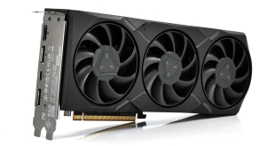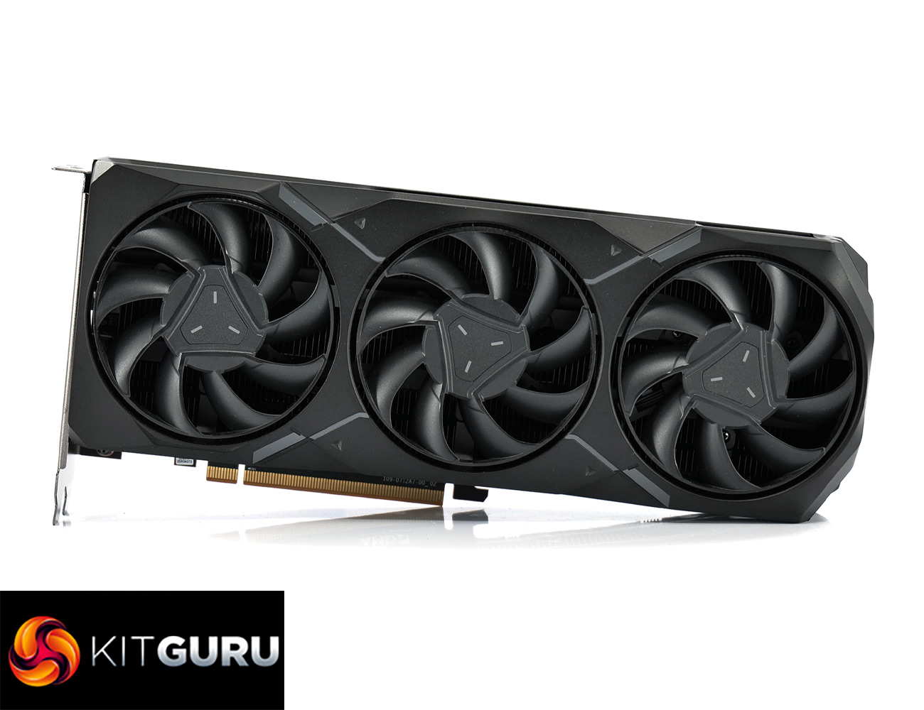
I have to be honest, today's review was not something I had on my radar in 2024. That's because we're taking a look at AMD's RX 7900 GRE graphics card, a product which first launched as an exclusive for the Chinese DIY market last July, before it eventually worked its way into the hands of system integrators. Today, however, AMD is announcing the worldwide availability of this GPU, alongside a new $549 price tag. We put it to the test and find out how it stacks up against the competition.
To put AMD's RX 7900 GRE into context, this GPU launched all the way back in July 2023 to little fan-fare, given it was originally sold as a China exclusive. That also explains the name, with GRE standing for Golden Rabbit Edition, as 2023 was the Year of the Rabbit. It's slightly ironic then that worldwide availability is happening now in 2024, the Year of the Dragon, but we digress… After its initial launch, the 7900 GRE began to be sold via system integrators in certain prebuilt PCs, and I even reviewed one such system from Cyberpower last November. Up until now though, it was only officially launched for the DIY market in China.
That changes today as AMD has announced worldwide availability for the RX 7900 GRE while also adjusting its price, given it first launched at $649 last year but will now be sold for $549. Clearly AMD feels it is well positioned to take on Nvidia's RTX 4070 Super, a product which has put significant pressure on AMD's Radeon division in the mid-range market segment since it launched last month.
In today's review then, we assess the RX 7900 GRE in its reference form, comparing it against a whole heap of products from both AMD and Nvidia, looking at rasterisation performance, ray tracing, power draw, efficiency and more…
If you want to read this review as a single page, click HERE.
| RX 7900 XTX | RX 7900 XT | RX 7900 GRE | RX 7800 XT | RX 7700 XT | |
| Architecture | RDNA 3 | RDNA 3 | RDNA 3 | RDNA 3 | RDNA 3 |
| Manufacturing Process | 5nm GCD + 6nm MCD | 5nm GCD + 6nm MCD | 5nm GCD + 6nm MCD | 5nm GCD + 6nm MCD | 5nm GCD + 6nm MCD |
| Transistor Count | 57.7 billion | 57.7 billion | 57.7 billion | 28.1 billion | 28.1 billion |
| Die Size | 300 mm² GCD
220 mm² MCD |
300 mm² GCD
220 mm² MCD |
300 mm² GCD
220 mm² MCD |
200 mm² GCD
150 mm² MCD |
200 mm² GCD
150 mm² MCD |
| Compute Units | 96 | 84 | 80 | 60 | 54 |
| Ray Accelerators | 96 | 84 | 80 | 60 | 54 |
| Stream Processors | 6144 | 5376 | 5120 | 3840 | 3456 |
| Game GPU Clock | Up to 2300MHz | Up to 2000 MHz | 1880 MHz | 2124 MHz | 2171 MHz |
| Boost GPU Clock | Up to 2500 MHz | Up to 2400 MHz | Up to 2245 MHz | Up to 2430 MHz | Up to 2544 MHz |
| ROPs | 192 | 192 | 192 | 96 | 96 |
| AMD Infinity Cache | 96MB | 80MB | 64MB | 64MB | 48MB |
| Memory | 24GB GDDR6 | 20GB GDDR6 | 16GB GDDR6 | 16GB GDDR6 | 12GB GDDR6 |
| Memory Data Rate | 20 Gbps | 20 Gbps | 18 Gbps | 19.5 Gbps | 18 Gbps |
| Memory Bandwidth | 960 GB/s | 800 GB/s | 576 GB/s | 624 GB/s | 432 GB/s |
| Memory Interface | 384-bit | 320-bit | 256-bit | 256-bit | 192-bit |
| Board Power | 355W | 315W | 260 W | 263W | 245W |
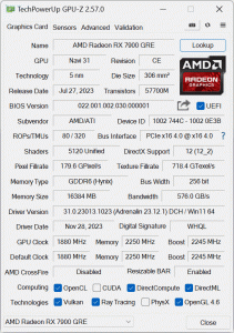
First, let's take a quick look at the specs. The RX 7900 GRE is using the same Navi 31 die that we first saw with the RX 7900 XTX and 7900 XT, but it has been significantly cut-down. Still, using the same die means we find a 300mm² Graphics Compute Die, based on TSMC's 5nm node, flanked by six 37mm² Memory Cache Dies (though two are disabled for the 7900 GRE). In total, the Navi 31 GPU packs 57.7 billion transistors.
While a full Navi 31 GPU packs in 96 Compute Units, the 7900 GRE is cut down to 80 CUs, 4 fewer than the 7900 XT, and each CU houses 64 Steam Processors, for a total of 5120 shaders. There's also 80 Ray Accelerators – one per CU – and 192 ROPs.
As for clock speed, AMD has de-coupled the clocks, so the front-end and shaders can operate at different clock speeds in a bid to save power. With the RX 7900 GRE, the shader clock features a rated game clock of up to 1880MHz, and a boost of up to 2245MHz, so that is a reduction of about 7% compared to the 7900 XT.
The memory configuration is where we see the biggest change compared to the 7900 XT, however. With two of the six MCDs disabled, the RX 7900 GRE packs 16GB of GDDR6 memory clocked at 18Gbps, operating over a 256-bit memory interface, for total memory bandwidth of 576 GB/s. 64MB of Infinity Cache is also present, which allows AMD to claim an ‘effective memory bandwidth' of up to 2265.6 GB/s.
Power draw for the RX 7900 GRE is also rated at 260W Total Board Power (TBP), but we are using our updated GPU power testing methodology in this review, so read on for our most detailed power and efficiency testing yet.
 KitGuru KitGuru.net – Tech News | Hardware News | Hardware Reviews | IOS | Mobile | Gaming | Graphics Cards


