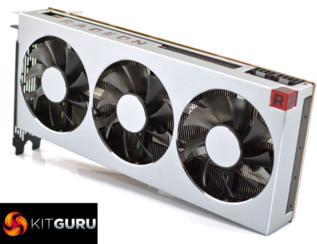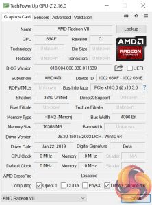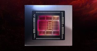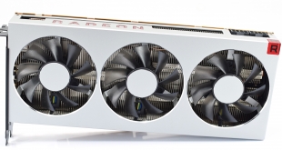
Following on from our unboxing earlier this week, the time has come where we can reveal performance figures for AMD's new high-end graphics card, the Radeon VII. Announced at CES 2019, the Radeon VII is the world's first gaming graphics card manufactured using a 7nm process. The GPU itself uses second generation Vega architecture, with a total of 60 compute units, 3840 stream processors and 64 ROPs – with 16GB of HBM2 memory sitting alongside. Is AMD back with a bang in the high-end market segment?
Aimed squarely at Nvidia's RTX 2080, AMD is no doubt hoping that its Radeon VII can capitalise on the relatively poor reception that Nvidia's Turing architecture has received from its consumer base. In terms of pricing, AMD yesterday confirmed a UK MSRP of £649. Speaking with Overclockers UK, too, they have confirmed stock will be available for £649.99 regardless of demand.
That puts the Radeon VII in very similar territory to the RTX 2080. Nvidia's Founders Edition RTX 2080 retails for £749, but aftermarket cards – including dual-fan factory overclocked solutions like this EVGA XC model – start at around £650 as well. How well does the Radeon VII compete with a 2080 in this situation? Let's find out.
| Radeon VII | RX Vega 64 | RX Vega 56 | |
| Architecture | Vega 20 | Vega 10 | Vega 10 |
| Manufacturing Process | 7nm | 14nm | 14nm |
| Transistor Count | 13.2 billion | 12.5 billion | 12.5 billion |
| Die Size | 331mm² | 495mm² | 486mm² |
| Compute Units | 60 | 64 | 56 |
| Stream Processors | 3840 | 4096 | 3584 |
| Base GPU Clock | 1400 MHz | 1274 MHz | 1156 MHz |
| Boost GPU Clock | 1750 MHz | 1546 MHz | 1471 MHz |
| Peak Engine Clock | 1800 MHz | 1630 MHz | 1590 MHz |
| Peak SP Performance | Up to 14.2 TFLOPS | Up to 12.7 TFLOPS | Up to 10.5 TFLOPS |
| Peak Half Precision Performance | Up to 28.1 TFLOPS | Up to 25.3 TFLOPS | Up to 21.0 TFLOPS |
| Peak Texture Fill-Rate | 432.24 GT/s | Up to 395.8 GT/s | Up to 330.0 GT/s |
| ROPs | 64 | 64 | 64 |
| Peak Pixel Fill-Rate | 115.26 GP/s | Up to 98.9 GP/s | Up to 94.0 GP/s |
| High Bandwidth Cache (HBM2) | 16GB | 8GB | 8GB |
| Memory Bandwidth | 1 TB/s | 483.8 GB/s | 410 GB/s |
| Memory Interface | 4096 bit | 2048 bit | 2048 bit |
| Board Power | 300W | 295W | 210W |
As is made abundantly clear by the Radeon VII's name, the big point about the Vega 20 architecture is that it is fabricated on TSMC's 7nm process. This has several consequences, including a die shrink – from 495mm² with Vega 64 to 331mm² for the Radeon VII, while the transistor count has increased from 12.5 billion to 13.2 billion. This also sees the addition of two extra HBM2 stacks (giving a total of 4x4GB stacks), with memory bandwidth coming in at a whopping 1 TB/s.
Elsewhere, clock speeds have been bumped up from the last-gen Vega cards. With Radeon VII, a 1750MHz boost clock is touted, with a ‘peak engine' clock of 1800MHz. It is important to note AMD defines the boost clock as ‘the typical achievable frequency in common workloads', meaning this is not a guaranteed speed – instead, consider it a ballpark figure for how fast your card should be running under load. We look at the actual real world clock speed later in the review.
Another interesting development with the Radeon VII comes from AMD's new thermal monitoring solution. With the new GPU, AMD has increased the total amount of thermal sensors spread across the chip to 64 – twice as many as Vega 64. This is coupled with AMD's move to control fan speed and thermal throttling via the Junction Temperature – the maximum temperature across the entire GPU die. AMD claims this allows for increased performance and ‘more dependable throttling', with the idea seeming to be that more accurate thermal information helps the GPU regulate its clock speed in a more consistent manner, so consistent speeds = steady frame rate.
One last thing to mention with the Radeon VII is the power draw. AMD rates the board power consumption at 300W, though it is interesting there is no secondary BIOS, or power profile available in Wattman, that manages the power draw to a lower level. With Vega 64, for instance, users could choose between either the Primary or Secondary V-BIOS (with the Primary BIOS having a higher TDP) and then either the ‘Balanced' or ‘Turbo' profiles within Wattman. With Radeon VII, there is only one ‘default' power state, unless you manually overclock.
 KitGuru KitGuru.net – Tech News | Hardware News | Hardware Reviews | IOS | Mobile | Gaming | Graphics Cards


