Intel officially announced its new 10nm ULP x86 microarchitecture – Tremont. This new microarchitecture will be at the core of Intel's Lakefield chipsets, planned to be used in servers, IoT devices, laptops, 5G networking, and tablets, like the Surface Neo.
Yesterday, in Santa Clara, California, at the Linley Fall Processor Conference, Intel introduced the new “Tremont” architecture. According to Stephen Robinson, Intel's Tremont Chief Architect, this is “Intel's most advanced low-power x86 architecture to date”. The new ULP (ultra low power) architecture will be used in the upcoming Atom processors, namely the Lakefield processors that will be used in Microsoft's Surface Neo.
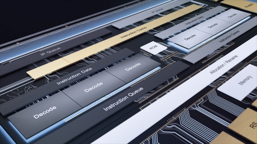
Compared to Tremont's predecessor, the Goldmont Plus, there's a 30% IPC performance boost, as a result of the design differences. Tremont will be using a branch prediction similar to the ones used in Intel's Core, using a 6-wide (2×3-wide clustered) decode engine accompanied by a 4-wide allocation/dispatch engine, while connected to 10 execution ports – 7 for integer execution and 3 for vector execution. The maximum L2 cache increased 0.5MB to 4.5MB, and the number of instruction sets increased by 8. All of this results in performance levels similar to Sandy Bridge in a mobile-centric package, according to WCFTech.
Tremont microarchitecture will bring a new technology called Intel Speed Shift, for fast ramp-up/down of high-frequency operation. It will also support Intel Total Memory Encryption, for “improved confidentiality protection in memory,” Intel's Boot Guard and Trusted Execution Technology, plus Rooted Secure Boot.
We will be able to see the new Tremont-based chips 2020.
KitGuru says: With the Ice Lake out in the wild, and this announcement, it seems that Intel's finally ready to go full 10nm. Although we know that the forthcoming Coffee Lake refresh is 14nm, maybe we don't have to wait much longer for a 10nm desktop platform. For now, let's just wait for the real-world benchmarks to see how good Tremont really is.
 KitGuru KitGuru.net – Tech News | Hardware News | Hardware Reviews | IOS | Mobile | Gaming | Graphics Cards


