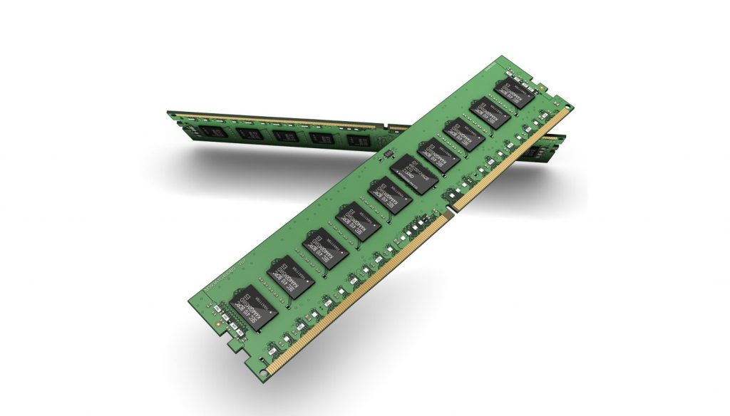
Samsung has announced today that is has successfully shipped one million DRAM modules manufactured from the industry’s first 10 nm-class (D1x) DDR4 extreme ultraviolet (EUV) technology.
The company claims that this will “open the door” to more industry-leading EUV process nodes for next-generation products to be used in premium PC, mobile, enterprise and datacentre systems. Samsung is said to have adopted the EUV manufacturing process in DRAM production to overcome the challenge of DRAM scaling.
“This major advancement underscores how we will continue contributing to global IT innovation through timely development of leading-edge process technologies and next-generation memory products for the premium memory market,” said Jung-bae Lee, executive vice president of DRAM Product & Technology at Samsung Electronics.
EUV manufacturing reduces repetitive steps in multi-patterning while also improving patterning accuracy to bring higher yields, greater performance and shorter development time. Samsung says that EUV manufacturing will be fully deployed in the future generations of its DRAM products, this will begin with either its fourth generation 10 nm-class (D1a) or 14 nm highly advanced DRAM.
Samsung is also expected to start volume production of the company’s D1a-based DDR5 and LPDDR5 in 2021, something that would double the manufacturing productivity of its 12-inch D1x wafers. In addition, To further address the growing industry demand for next-generation premium DRAM, Samsung is expected to open operation of a second semiconductor fabrication line at its plant in Pyeongtaek, South Korea later this year.
KitGuru says: Due to the increased demand for next-generation chips from various areas of the industry, Samsung is stepping up EUV production at its fabrication plants to accelerate the transition to DDR5 and LPDDR5 in the near future.
 KitGuru KitGuru.net – Tech News | Hardware News | Hardware Reviews | IOS | Mobile | Gaming | Graphics Cards


