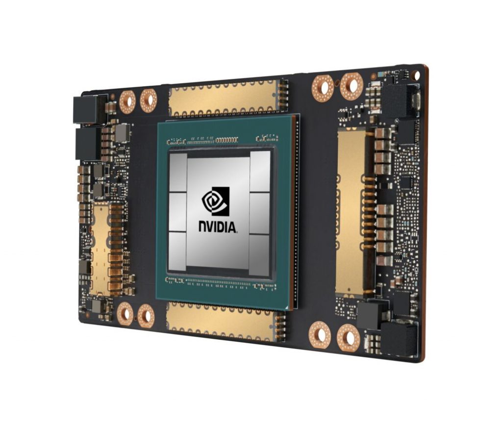
After some back and forth, today Nvidia officially uploaded its big GTC reveals in a series of videos presented by CEO, Jensen Huang. The biggest announcement of the day was the A100 GPU, powered by the new Ampere architecture.
Ampere will be coming to GeForce series graphics cards eventually, but for now, Nvidia is focusing purely on professional markets, including AI, data-centres and cloud. Kicking off the rollout of the Ampere architecture is the A100 family of GPUs, boasting nearly 20 TFLOPS of performance.
The A100 is the successor to the Volta-based V100, upgrading to TSMC's 7nm process and packing 54 billion transistors, more than double the transistor count found in the V100. For single-precision applications, the A100 has 19.5 TFLOPS of compute performance, and 9.7 TFLOPS in single-precision.
The machine learning accelerating Tensor Cores deliver even more, reaching 312 TFLOPS in FP16 Tensor workloads. In terms of memory, you are looking at 40GB of HBM2 with 1.6TB/s of bandwidth, the CUDA core count has also risen to 6912.
It is a more power hungry GPU compared to the V100 though, with a TDP of 400W rather than 350W.
We will be getting more details on Ampere in the months ahead. We don't know when this new architecture will make its way over to GeForce GPUs, but it should bring a nice performance uplift. You can see Nvidia's full video presentation on the A100, HERE.
KitGuru Says: Did any of you watch the Nvidia presentations released today? What do you think of the new Ampere architecture so far?
 KitGuru KitGuru.net – Tech News | Hardware News | Hardware Reviews | IOS | Mobile | Gaming | Graphics Cards


