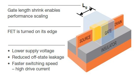
GlobalFoundries has announced that its 12nm FinFET technology is ready for production. According to the company, the technology is “optimised for AI Accelerator Applications” and “ideal for high-performance, power-efficient SoC applications” .
GlobalFoundries 12nm FinFET technology is manufactured at facilities in Saratoga County, New York and is set to be used in “Computing, Networking, Mobile and Server applications”. The company said that the “12LP technology can provide up to 75% higher device performance and 60% lower total power” compared to 28 nm. GlobalFoundries also said that the 12nm FinFET technology is streamlined for artificial intelligence (AI) training and inference applications.
Image credit: GlobalFoundries
“Artificial intelligence is on a trajectory to become the most disruptive technology of our lifetime,” said Amir Faintuch, senior vice president and general manager of Computing and Wired Infrastructure at GF.
“It is increasingly clear that the power efficiency of AI systems – in particular how many operations you can wrest from a watt of power – will be among the most critical factors a company considers when deciding to invest in data centres or edge AI applications. Our new 12LP+ solution tackles this challenge head-on. It has been engineered and optimised, obsessively so, with AI in mind.”
GlobalFoundries has released some more in-depth documentation explaining this new tech, which you can find HERE.
KitGuru says: It feels like AI is making its way into almost every computer related product nowadays. What changes do you think that AI will bring about?
 KitGuru KitGuru.net – Tech News | Hardware News | Hardware Reviews | IOS | Mobile | Gaming | Graphics Cards


