

Today Intel has revealed its roadmap of process and packaging improvements, which will power the next several generations of Intel CPUs leading up to 2025 and beyond. This includes Intel's first new transistor architecture in more than a decade.
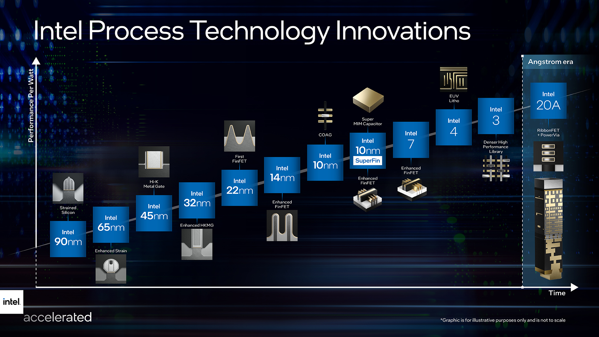
The new roadmap includes Intel's updated node naming structure, which aims to “give customers a more accurate view of process nodes across the industry”. The roadmap includes four upcoming nodes – Intel 7, Intel 4, Intel 3 and Intel 20A.
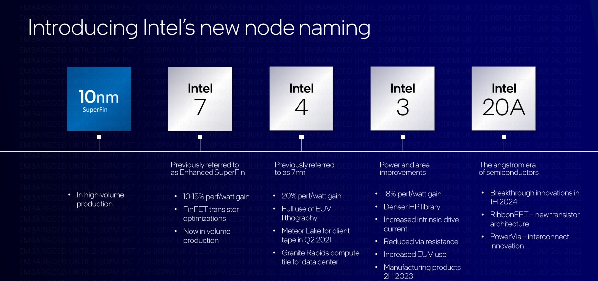
As you can see in the slide above, Intel 7 will deliver a 10 to 15 percent performance-per-watt increase compared to Intel 10nm SuperFin. We'll see this node rolling out on Alder Lake client CPUs in 2021, and Sapphire Rapids for data centre. Intel 4 will see the company fully embrace EUV lithography, delivering around 20 percent more performance-per-watt in 2022. Intel 3 will further increase EUV to deliver an additional 18 percent performance-per-watt increase over Intel 4 – this will also be Intel's last FinFET based processor, currently targeting a H2 2023 launch.
In late 2024-2025, Intel will be launching Intel 20A, ushering in the ‘angstrom era' with two new technologies – RibbonFET and PowerVia. The former is Intel's gate-all-around transistor technology, the first new transistor architecture from Intel since introducing FinFET in 2011. Improvements will include faster transistor switching speeds at higher efficiency. This architecture will also introduce PowerVia, an industry-first implementation of backside power delivery to further optimise signal transmission by removing the need for power routing on the front side of the wafer.
These new processors will also see the introduction of new packaging technologies. Intel has detailed three of them today:
- Foveros – wafer-level packaging capabilities to provide a first-of-its-kind 3D stacking solution. Meteor Lake will be the second generation implementation of Foveros in a client product and features a bump pitch of 36 microns, tiles spanning multiple technology nodes and a thermal design power range from 5 to 125W.
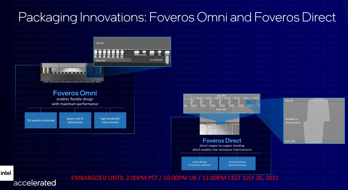
- Foveros Omni – Provides unbounded flexibility with performance 3D stacking technology for die-to-die interconnect and modular designs. Foveros Omni allows die disaggregation, mixing multiple top die tiles with multiple base tiles across mixed fab nodes and is expected to be ready for volume manufacturing in 2023.
- Foveros Direct – direct copper-to-copper bonding for low-resistance interconnects and blurs the boundary between where the wafer ends and where the package begins. Foveros Direct enables sub-10 micron bump pitches providing an order of magnitude increase in the interconnect density for 3D stacking, opening new concepts for functional die partitioning that were previously unachievable. Foveros Direct is complementary to Foveros Omni and is also expected to be ready in 2023.
These technologies will primarily be developed at Intel's labs in Oregon and Arizona. Over these next four years, Intel believes these technologies will bring the company back to process performance leadership.
Discuss on our Facebook page, HERE.
KitGuru Says: This is a pretty packed roadmap, so Intel will be moving rapidly over the next few years. Now we'll just have to wait and see them deliver.