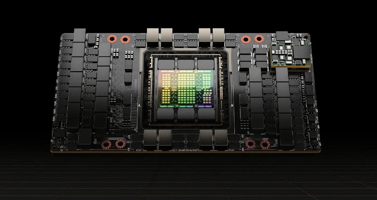
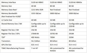
Today at GTC, Nvidia officially unveiled its new GPU architecture, Hopper. The first Hopper GPU will be none other than the H100, based on a custom TSMC 4nm node, packing 80 billion transistors, up to 80GB of HBM3 memory and up to 700W TDP.
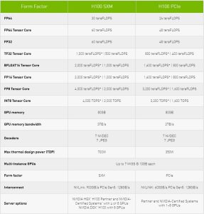
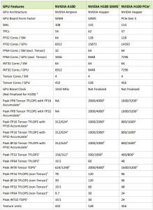
During the keynote, Nvidia promised huge performance gains from the H100. The GPU will be available in two forms, an SXM version and a standard PCIe version. The GPU should offer 3x more compute performance in FP64, TF32 and FP16 compared to the A100, as well as 1.5x more memory bandwidth.
In the gallery above, you can see the full spec sheet for the H100, as well as a page detailing TFLOP, TOPS and FLOPS ratings for different cores. The SXM version is the more powerful of the two, with a 700W TDP, more memory bandwidth and higher performance, the PCIe Gen 5 version has a 350W TDP by comparison.
Nvidia DGX H100 systems, as well as DGX PODs and SuperPODs with multiple GPUs, will be available via Nvidia partners in Q3 2022. Nvidia is also expected to launch its next-gen GeForce graphics cards in Q3 or Q4 2022, which will use a different GPU architecture (lovelace).
Discuss on our Facebook page, HERE.
KitGuru Says: What do you all think of the Hopper reveal from Nvidia?
 KitGuru KitGuru.net – Tech News | Hardware News | Hardware Reviews | IOS | Mobile | Gaming | Graphics Cards


