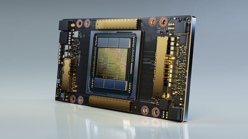
Nvidia is set to host its GTC keynote today and sure enough, it looks like we'll be seeing the new Hopper GPU architecture unveiled. Ahead of the keynote, presentation slides have leaked detailing the upcoming Nvidia H100 GPU, based on a custom 4nm node.
VideoCardz has posted what appear to be legitimate presentation slides from the upcoming keynote. The slides detail the specifications for the Nvidia H100 GPU, the first Hopper-based GPU, built using a custom TSMC N4 process technology and 80 billion transistors.
We are still awaiting full specs for the GPU, so we don't know how many CUDA Cores it has. However, we do know that it will feature up to 80GB of HBM3 memory with a 5120-bit bus, capable of 3TB/s of bandwidth – a 1.5x improvement over the previous A100. The graphics accelerator will use the PCIe Gen 5 interface, or the SXM form factor. The SXM version will have a maximum TDP of 700W.
Performance-wise, the H100 should offer 3x more compute performance in FP64, TF32 and FP16 compared to the A100, while consuming up to 300W more power. Nvidia's GTC keynote takes place this evening, so expect more details very soon.
Discuss on our Facebook page, HERE.
KitGuru Says: It is worth noting that Hopper will likely be reserved for professional and datacentre markets, while ‘Lovelace' will be the next GeForce graphics architecture. We should get more news on next-gen GeForce GPUs in Q3 or Q4 this year.
 KitGuru KitGuru.net – Tech News | Hardware News | Hardware Reviews | IOS | Mobile | Gaming | Graphics Cards


