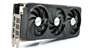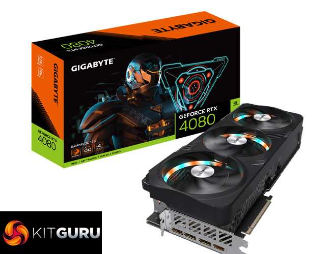
Following on from our day-1 review of the Nvidia RTX 4080 Founders Edition, today we are back with a look at our first AIB model. Enter the Gigabyte RTX 4080 Gaming OC. If it looks familiar, Gigabyte has not changed much from the RTX 4090 Gaming OC that we reviewed a few short weeks ago, but what does that mean for the smaller AD103 silicon? We test thermals, acoustics, overclocking and more to find out.
While the shroud and size of the Gigabyte RTX 4080 Gaming OC may appear identical to that of the RTX 4090 Gaming OC, it's interesting to note that there are actually some differences between the two. For one, the RTX 4080 actually has an extra heatpipe – an interesting decision considering the 4080 is a lower power GPU. The PCB has also been tweaked, with a cut-back VRM compared to the RTX 4090.
We still find a huge, 3.5 slot design however, as well as dual-BIOS, a 30MHz factory overclock and an increased power limit. Let's find out how the Gaming OC compares to the Founders Edition.
| RTX 4090 | RTX 4080 | RTX 3090 Ti | RTX 3090 | RTX 3080 Ti | RTX 3080 | |
| Process | TSMC N4 | TSMC N4 | Samsung 8N | Samsung 8N | Samsung 8N | Samsung 8N |
| SMs | 128 | 76 | 84 | 82 | 80 | 68 |
| CUDA Cores | 16384 | 9728 | 10752 | 10496 | 10240 | 8704 |
| Tensor Cores | 512 | 304 | 336 | 328 | 320 | 272 |
| RT Cores | 128 | 76 | 84 | 82 | 80 | 68 |
| Texture Units | 512 | 304 | 336 | 328 | 320 | 272 |
| ROPs | 176 | 112 | 112 | 112 | 112 | 96 |
| GPU Boost Clock | 2520 MHz | 2505 MHz | 1860 MHz | 1695 MHz | 1665 MHz | 1710 MHz |
| Memory Data Rate | 21 Gbps | 22.4 Gbps | 21 Gbps | 19.5 Gbps | 19 Gbps | 19 Gbps |
| L2 Cache | 73729 KB | 65536 KB | 6144 KB | 6144 KB | 6144 KB | 5120 KB |
| Total Video Memory | 24GB GDDR6X | 16GB GDDR6X | 24GB GDDR6X | 24GB GDDR6X | 12GB GDDR6X | 10GB GDDR6X |
| Memory Interface | 384-bit | 256-bit | 384-bit | 384-bit | 384-bit | 320-bit |
| Memory Bandwidth | 1008 GB/Sec | 716.8 GB/Sec | 1008 GB/Sec | 936 GB/Sec | 912 GB/Sec | 760 GB/Sec |
| TGP | 450W | 320W | 450W | 350W | 350W | 320W |
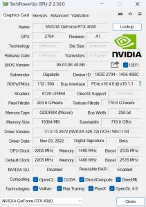
First, for a quick spec recap. RTX 4080 uses the AD103 die, and this is notably smaller than AD102, measuring 378.6mm2. Accordingly, transistor count is reduced from 76.3 billion, down to 45.9 billion. The fundamental building blocks are still the same of course, with the RTX 4080 offering a total of 84 Streaming Multiprocessors (SMs), each housing 256 CUDA Cores, for a total of 9728. We also find 84 RT cores, 336 Tensor cores, 336 Texture Units, and 112 ROPs.
TSMC's N4 node has Nvidia cranking up the clock speed significantly this generation, with the RTX 4080 sporting a 2505MHz rated boost clock. Gigabyte has increased this further with a 30MHz factory overclock.
The memory configuration is another area where AD103 has been cut-back significantly. The memory interface has been reduced to 256-bit, and even with 16GB GDDR6X running at 22.4Gbps, that cuts memory bandwidth down to 716.6GB/s. That said, there has been a substantial upgrade to the L2 cache with the Ada architecture, with the RTX 4080 now offering 65.5MB, compared to just 6MB for GA102.
Considering RTX 4080 is notably cut-down versus the RTX 4090, rated power draw is lower, with a 320W TGP. Gigabyte has bumped this up slightly however, with a 340W limit for the Gaming OC.
 KitGuru KitGuru.net – Tech News | Hardware News | Hardware Reviews | IOS | Mobile | Gaming | Graphics Cards


