SK hynix say that the SH920/910A range of SSD products is good for embedded and server solutions. The claimed average time between failures (MTBF) is put at 1.2 million hours, a little shy of the Toshiba HG6 that we looked at in March, but still seriously reliable.
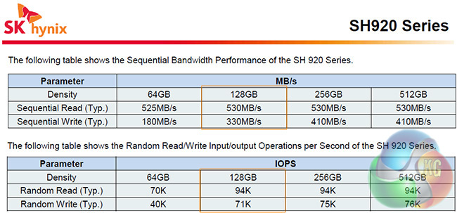
Claimed performance is 530MB/sec read and 330MB/sec write with the 128GB version, but SK hynix says that the write speed will peak closer to 410MB/sec on the 256GB and 512GB capacity drives. Be aware that the smallest 64GB model has reduced sequential write speeds around 180 MB/s.
The IOPS results also look to scale with capacity, which makes it a little strange that SK hynix have chosen to begin sampling on a drive that is ‘less than the fastest in the range'. That said, price points are a key factor and maybe that was a more important consideration when it comes to making an impact at launch.
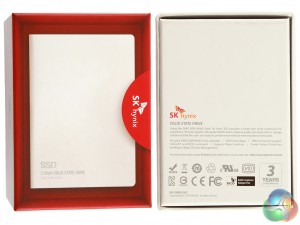
SK hynix sent us one of the only full retail boxed products available. Here we go with a look at the consumer-friendly packaging. Remember, click on the image to get a larger version that you can investigate more fully.
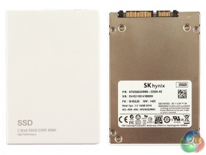
One thing we realised straight away is that it is not easy to understand which drive you are looking at. Maybe there will be a sticker of some sort when it arrives on the shelves, but on our review sample there was no obvious, or visible SH9xx logo.
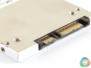
The clean, white units seem professional and functional. We thought the inclusion of multiple pre-threaded screw holes was strange, given that this model was physically sealed with no screws visible. That said, if a company can use the same shell for a number of products, then maybe these additional holes give manufacturing flexibility. The white shell makes it seem Apple-friendly and when we spoke with the head of sales for SK hynix in our region, he said that they expect the drive to have universal appeal.
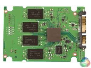
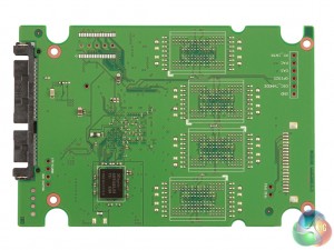
After some careful work on the outer shell, the SSD gave up its inner secrets.
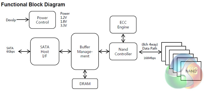
Internally, the SSD is set up using a SOC (System On a Chip) design. This is a cost effective way to manage the 6Gb/sec from multiple flash memory devices on multiple channels. It has an 8 channel, 4-way data path.
The NAND itself is 20nm MLC, designed and built by SK hynix themselves. The DRAM shown is a cache, which varies in size according to the storage capacity of the SSD unit. The 128 and 256GB versions have 2GB here, while the 512GB version has double that.
Here's another interesting section from Hynix's documentation. It shows the expected performance levels. It will be interesting to see how the speeds that SK hynix officially quote actually map out in KitGuru's testing later on in this review.
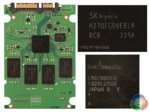
Clicking on this image will give you the specific chip details from our model. We removed the small sticky ‘buffer pad' to get the center chip shot.
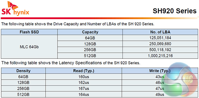
One last snapshot from the SK hynix documentation. Let's have a look at how latency and capacity also vary by model.
While the difference in number from row to row might not change much, every small change does have an impact on measured speed.
Will that measured difference be perceptible in the real world? Now that's a different question.
 KitGuru KitGuru.net – Tech News | Hardware News | Hardware Reviews | IOS | Mobile | Gaming | Graphics Cards



great upgrade for a lower end laptop.
I just scanned this review 2 times and can’t find a mention of what controller is used in this thing. Is it under that pad in image 4 four or do I need a better microscope? Omitting that major data point makes for a very strange review.