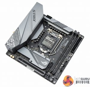
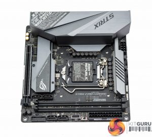
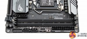
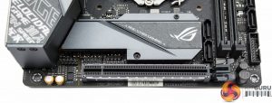
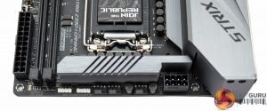
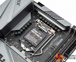
The aesthetics of the ASUS ROG Strix Z390-I Gaming have distinctively evolved from the Z370-I and Z270i predecessors. The overall look is smart, with a neutral colour palette, and makes good use of heatsinks and an I/O cover to deliver visual appeal that is typically difficult to achieve on such a small motherboard.
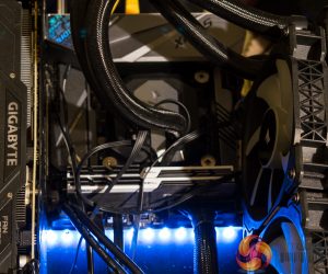
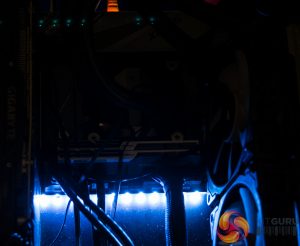
The primary onboard RGB lighting zone runs underneath the motherboard 24pin and is fully customisable using the ASUS AURA software. Up to two more RGB strips can be added, through 5v Digital Addressable and 12v headers respectively, for those system builders with a taste for customisation.
ASUS packs in a MemOK! switch, MemOK! LED and full debug LEDs to assist with the building and troubleshooting process. A front panel USB 3.1 header and a cooled M.2 slot are also welcomed additions.
The location of the front panel, USB 2.0 and HD audio connections is somewhat awkward, sandwiched right in between the PCIe lane and the M.2 heatsink. That said, ASUS does provide a front panel extension cable to make the installation of those front panel connections a little easier.
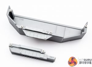
A pair of heatsinks for the CPU VRM should keep thermals under control, many motherboards vendors have been known to sacrifice one of these heatsinks when space or cost limitations become tricky.
The I/O shield is fully integrated into the motherboard design, simplifying the building experience. Overall connectivity is impressive with two 4K-capable display outputs and 7 USB ports spanning Type-C and all USB generations of recent times. The integrated WiFi, now a default part of the Z390 chipset, is a nice addition for those who are unable to make use of wired networking connectivity.
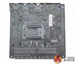
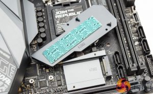
Underneath the motherboard is a second M.2 slot, without any cooling.
The primary M.2 slot features some cooling but that heatsink assembly is shared with the chipset so it remains to be seen how effective the cooling might be.
The rear I/O cover, impressively, is metal in its entirety so all of it represents cooling surface area for the VRMs. The VRM heatsink and I/O cover merge into a single piece.
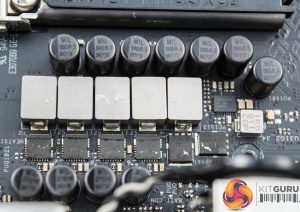
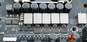
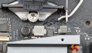
The configuration of the VRM is not immediately clear from the pictures but there are a significant number of components on show. There are 11 full-sized inductors, 8 ON Semiconductor 302045 integrated MOSFET and driver packages (i.e. include the high- and low-sides, and driver in the same chip), a further two ON Semiconductor MOSFETs (NTMFS4C10N, NTMFS4C06N) and a custom ASUS VRM controller (ASP1401CTB).
The exact configuration is not specified but ASUS does provide 6 phases worth of CPU VRM components, using 3 PWM signals which is a technique it calls “twin phases”, and then a further 2 phases worth iGPU VRM components, likely with 2 PWM signals. Then there are a few other ancillary phases around the CPU VRM for things like the VCCSA and VCCIO which give the illusion of a greater number of phases.
The summary is that it is most likely a 6+2+1+1 “virtual” configuration of VCore + VCCGT (iGPU) + VCCSA + VCCIO, 3+2+1+1 “actual”.
To even call it “6 phases” at all for the VCore is slightly misleading given there are no doublers at play but it really depends on how flexible the definition of a phase is.
ASUS claims improved transient response and less voltage droop between load switching, compared to doubler based solutions.
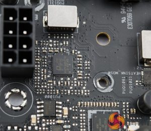
The PWM controller is marked ASP1401CTB and is thought to be a unit capable of up to 4+2 phases, but in this configuration it is likely operating as 3+2 phase.
All the inductors/chokes used are solid units and the capacitors are 5,000 (5K) hours rated units, marked “MIL 560/6.3 5KY17 or 5KY19”.
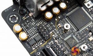
The audio section features PCB isolation with the codec hiding in between the rear I/O items. There are gold audio series capacitors as well as two operational amplifiers, both by Texas Instruments – OPA1688 and R4580I.
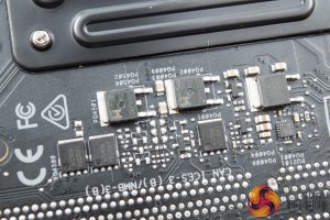
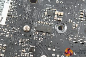
There are some more VRM components underneath the motherboard, potentially supporting the memory VRMs.
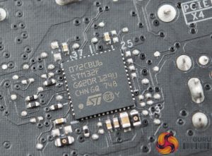
An STMicroelectronics STM32F 072CBU6 ARM microcontroller is located on the back, though we're not sure what it is in charge of controlling.
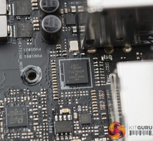
A Parade PS175HDM chip is in charge of providing the HDMI 2.0 connectivity at the rear I/O.
Two Texas Instruments TPS51362 Synchronous converters are used. The vendor says they are designed for VCCIO and DDR voltage applications.
The Pericom P13EQX chip is used as a redriver for the USB 3.1 (10Gbps) signal available on the rear I/O.
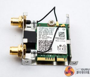
The WiFi module is provide by Intel's Wireless-AC 9560NGW chipset, which combines Bluetooth 5.0, and sits on the Intel integrated connectivity (CNVi) interface.
 KitGuru KitGuru.net – Tech News | Hardware News | Hardware Reviews | IOS | Mobile | Gaming | Graphics Cards


