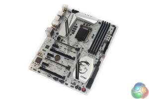
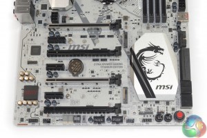
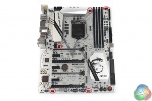
Its unique appearance is the first noteworthy point for the MSI Z170A XPower Gaming Titanium Edition motherboard. Despite appearing to be white in many pictures, the board has more of a subdued metallic aura to it. I use the word subdued because the eight-layer PCB is far from the reflectiveness of a material such as aluminium foil.
The heatsinks are noticeably more shiny and feature a finish that resembles powder coating, with the appearance of fine metallic particles being present. There is no rear IO port cover that we have seen utilised on many other gaming motherboards. Overclocking users told MSI that IO covers simply get in the way when pushing the board with extreme cooling hardware so the company decided against providing one.
This may not be a move that many general enthusiasts interested in system appearance will appreciate.
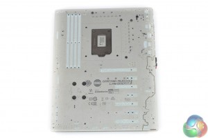
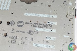
Taking a look at the board's rear side allows the PCB colour to be characterised more effectively. The metallic-looking coating seems to be applied over a white PCB layer positioned underneath. Cut-outs near many connectors provide this indication.
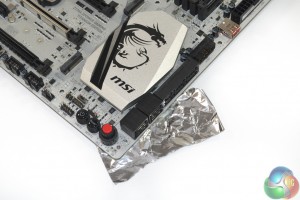
Along the board's upper-right edge are the 24-pin power connector, a right-angled USB 3.0 Type-A port, the OC Dashboard header, and voltage reading points. The right-angled USB 3.0 header delivers two 5Gbps ports directly from the Z170 chipset. Two ASM1464 re-drivers are used to boost the USB 3.0 port output signals for use with long chassis front panel cables.
MSI also allocates an onboard flashback button that can be used with the dedicated BIOS Flashback+ USB port in order to update the BIOS without components (such as a CPU) installed.
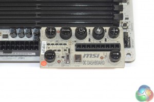
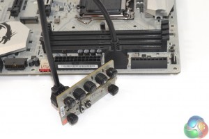
MSI's OC Dashboard is able to sit directly on the motherboard or it can be positioned elsewhere thanks to the included cable. That latter point is useful for sub-zero overclockers because the memory slots regularly freeze during an extended session of even CPU-only LN2 benching.
The allocated buttons allow for increases and decreases to the CPU multiplier and BCLK, as well as simple power and reset functionality. The discharge button can be used to completely wipe all previously-applied settings from the motherboard – think of it as a more in-depth clear CMOS tool.
There are also headers to enable slow mode, which is useful when you need to push the system and not worry about it crashing before you've saved your benchmark screenshot. And the ‘FASTB1‘ button can be used to boot directly into the UEFI. It is good to see that access to the V-Check points is maintained – competitive overclockers will always use a multimeter rather than rely on software to tell voltage readings.
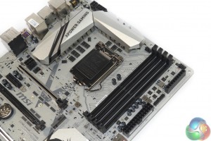
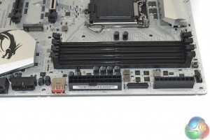
Four single-latch DIMM slots provide support for up to 64GB of DDR4 memory in dual-channel mode, with MSI stating frequency support of up to 4000MHz via overclocking (although higher may be obtainable, depending on the CPU's IMC strength). The board uses isolated circuitry for the memory paths in order to minimise signal interference, and this seems to have worked based on a DDR4 frequency world record that the Z170A XPower Titanium has previously taken.
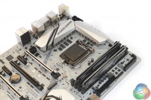
Central to the board is its standard LGA1151 CPU socket. No fancy LGA 2011v3-esque pin enhancements here, just a standard socket that is fed by an 8-pin and a 4-pin power connector to provide ample power for an overclocked Skylake CPU.
It is worth highlighting how clean and unobtrusive the CPU socket area is. MSI makes use of numerous low-profile Hi-C capacitors rather than the standard, tall can-style capacitors. This helps to minimise interference around the CPU socket when using large CPU air coolers, or more importantly, when trying to insulate the socket area for use with sub-zero cooling techniques.
Large capacitors poking out present insulation and protection headaches for sub-zero users trying to effectively apply artist's rubber and Vaseline around the socket area.
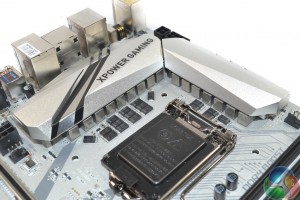
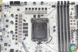
The sixteen-phase power delivery system is formed of MSI's Military Class 5 components – Titanium chokes, DrMOS (driver MOSFETs), Hi-C (low profile) capacitors, and aluminium-core Dark capacitors. Marketing claims aside, Titanium chokes are indeed useful thanks to their higher inductance density than ferrite-core alternatives, higher service temperature, and enhanced lifespan.
MSI's sturdy (!) metal heatsink is connected via a heatpipe and directly cools the MOSFETs as well as the chokes. That latter point is rather unusual, but additional cooling for the inductors is welcomed.
Beneath the heatsink are 14 of International Rectifiers' highly-respected IR3555M PowIRstages each rated for a 60A current capacity. The modules integrate MOSFETs with a Schottky diode and driver IC (hence MSI's DrMOS or ‘DriverMOS' name) onto a single solution that saves on PCB space. The IR3555M solutions are some of the best power delivery MOSFET packages available to motherboard vendors.
Assisted by seven rear-mounted International Rectifiers IR3599 phase doublers is the same vendor's IR35201 PWM controller which features up to eight control channels. Two Powervation PV3205 controllers and a cluster of high- and low-side MOSFETs handle non-CPU power duties.
An IDT 6V41516NLG clock generator is used to manage the BCLK flexibility that Skylake CPUs are permitted.
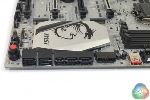
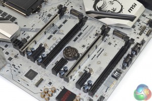
On the storage front, the board is equipped with a pair of SATA-Express ports that use PCIe 3.0 x2 lanes from the Z170 chipset in order to provide a bandwidth of 16Gbps. While no current SATA-Express devices make use of such bandwidth, the speed is useful for application with front panel USB 3.1 ports, many of which currently use the SATA-E connector.
A total of eight SATA 6Gbps ports are provided, six of which come from the Z170 chipset (four deployed in the SATA-Express connectors) with the remaining pair being provided by ASMedia's slower ASM1061 controller (use these for slower drives). All of the standard RAID modes are supported by the Z170-fed ports. SATA ports 7 and 8 are powered by ASMedia – MSI's onboard markings do not make this clear, however the manual does.
Two 32Gbps (PCIe 3.0 x4) M.2 connectors are used on the board, both of which are positioned beneath important PCIe slots typically used by graphics cards. While I like the logic of hiding an ugly green M.2 SSD beneath a graphics card, there are some thermal concerns with the positioning. There also seem to be interference issues if using a U.2 adapter that fits into the M.2 slot, although I do not have the relevant adapter to confirm this.
The M.2 connectors also support SATA 6Gbps and older PCIe 2.0 x2 SSDs using the M.2 form factor. RAID 0 and 1 are supported for the M.2 ports and a bootable volume can be created thanks to Intel's latest RST iteration with the Z170 chipset.
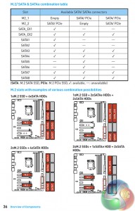
Analysing which ports can and cannot be used together is a serious headache due to the flexible nature of the 26 high-speed IO lanes on Intel's Z170 chipset (it took me about 10 minutes and a couple of back-of-the-envelope block diagrams to decode MSI's implementation).
Thankfully, the vendor includes a convenient table and images showing possible usage distributions for storage devices. For example, a pair of high-speed PCIe 3.0 x4 SSDs could be used in RAID 0 while also running a USB 3.1 front panel implementation through SATA-Express and maintaining the pair of ASM1061 SATA 6Gbps ports for slower storage drives.
It is storage distributions such as the example listed above that make the added pair of ASM1061 SATA 6Gbps ports such a useful addition, despite their inferior performance.
Four full-length PCIe slots are found on the board, however only two run at a minimum of PCIe 3.0 x8 bandwidth due to a mixture of the limited number of CPU lanes available and MSI's allocation of the chipset resources. These two will be the prime candidates for graphics card usage and are therefore reinforced with steel to prevent damage and mitigate EMI.
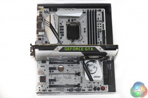
Slot spacing is good for two-card usage, although there is little more than a millimetre of clearance between a Noctua NH-D14 and a GTX 980 Ti in the first PCIe slot. Cards with a thick backplate are likely to contact wide CPU coolers, so this should be accounted for at the component selection stage. A 6-pin PCIe power connector is provided for assisting with power-hungry expansion duties.
The four slots can be allocated as PCIe 3.0 x16/x0/x0/chipset x4, x8/x0/x8/chipset x4 or x8/x4/x4/chipset x4. While you can technically run 3- and 4-way CrossFire (SLI demands x8 connections), you're only realistically going to want to use up to two graphics cards in a multi-GPU configuration, both of which can be delivered PCIe 3.0 x8 bandwidth from the CPU's sixteen on-chip lanes.
That lowermost full-length slot uses four PCIe 3.0 lanes from the Z170 chipset and shares them with the three neighbouring PCIe 3.0 x1 slots. This is good to see because it means that a high-bandwidth PCIe 3.0 x4 device (RAID card, 10Gbps NIC, Intel 750 SSD) can be used alongside two graphics cards running at x8/x8, without interfering with the M.2 and SATA-Express allocation.
Albeit highly unlikely, storage geeks wanting a high-performance workstation or content creation server could go crazy with this board. There's the room, and appropriate lane distribution, for four PCIe 3.0 x4 add-in cards (Intel SSD 750 drives or high-bandwidth RAID cards, for example), two PCIe 3.0 x4 M.2 SSDs, as well as one PCIe 3.0 x2 SATA-Express device, in addition to the pair of ASMedia SATA 6Gbps ports. The Skylake chip's iGPU would handle video output duties.
We see the standard USB 2.0, front panel, and audio headers along the board's bottom edge. MSI also deploys a number of overclocker-centric features in this area, which is far from the vicinity of potentially sub-zero graphics cards.
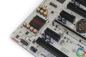
The two-digit POST LEDs display temperature when the system is running in an OS. Next to the display is the switch box that allows PCIe slots one, two, and three to be disabled for troubleshooting measures. Moving to the right side sees onboard power, reset, and auto OC dial deployed.
Slightly below the chipset heatsink is the pair of BIOS chips as well as the selection switch. I am glad to see MSI utilising dual BIOS chips for an overclocking-geared motherboard as this approach provides redundancy against BIOS crashes.
MSI's Audio Boost 3 system is based around the Realtek ALC 1150 codec. Two Texas Instruments OP1652 operational amplifiers are used to drive high-impedance headphones. Nippon Chemi-Con audio capacitors are also utilised.
EMI reduction is conducted by carrying the audio signals along segregated PCB paths, covering the Realtek codec, and using gold-plated audio jacks.
Nahimic audio software is provided for use inside the operating system.
In a somewhat surprising move, MSI equips the board with Intel's I219V NIC, rather than a Killer variant that we typically see on the vendor's Gaming motherboards. This is likely related to the inclusion of MSI's own network control software which effectively renders the Killer Network Manager software redundant (Killer's software is one of its NICs' biggest selling points). Intel's NICs typically operate with a lower CPU overhead which is useful for overclockers.
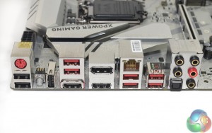
A PS/2 port is good to see for troubleshooting purposes. The rear clear CMOS button is another addition that I love to see and is something I deem a necessity on an overclocking geared motherboard. MSI allocates a Gaming Device Port for mouse management inside the OS. There are a total of three USB 2.0 ports (one of which is allocated BIOS Flashback duties) and four USB 3.0 ports on the rear IO, all of which stem from the Z170 chipset.
Two 10Gbps USB 3.1 Type-A ports (between the LAN and audio jacks) are provided by an ASMedia ASM1142 host chipset. There's no USB 3.1 Type-C connector as that would require additional cost (in the form of an EtronTech EJ179V switch IC) and is deemed irrelevant for an overclocking-geared board. The up-and-coming connection will be sorely missed by many general buyers, even if its 100W power delivery specification was not implemented (as it is not on most motherboards).
Onboard video takes the form of two HDMI ports which seem to be v1.4 (limited to 4096×2160@24Hz), as well as a DisplayPort output capable of 4K (3840×2160) at 60Hz.
As a side note, ignore MSI's stupid advertising of ‘USB 3.1 Gen 1‘ and ‘USB 3.1 Gen 2‘ ports. USB 3.1 Gen 1 is basic old USB 3.0 – 5Gbps. USB 3.1 Gen 2 is the new USB 3.1 connection that we are seeing emerge – 10Gbps. While MSI is not the only hardware vendor to use this frustrating advertising method, the approach infuriates me and is simply used to confuse consumers in my opinion.
Five 4-pin fan headers are scattered smartly around the board, two of which are allocated CPU control duties. Nuvoton's NCT6793D-M manages the fan control and hardware monitoring.
The board's unique styling and colour scheme are a solid match for metallic silver components such as a reference Nvidia graphics card and Crucial's Ballistix memory modules. White hardware would also be a good match, as would the contrast provided by black.
 KitGuru KitGuru.net – Tech News | Hardware News | Hardware Reviews | IOS | Mobile | Gaming | Graphics Cards



Allow me to show ~you a genuine way to earn a lot of extra money by finishing basic tasks from your house for few short hours a day — See more info by visiting >MY*&___(DISQUS)*%___ID)
I think you should do some reading before using harsh terms such as “stupid advertising”, perhaps you might even learn something new 😉
https://en.wikipedia.org/wiki/USB#USB_3.1
” The USB 3.1 standard increases the data signaling rate to 10 Gbit/s in the USB 3.1 Gen2 mode, double that of USB 3.0 (referred to as USB 3.1 Gen1)”
The information in that article, the referenced technical documents for which I have examined many times over the past year, says what I have said in the article. ‘USB 3.1 Gen 2’ is 10Gbps. USB 3.0 is 5Gbps and is sometimes referred to as ‘USB 3.1 Gen 1’ (by many vendors, not just MSI, as I clearly pointed out in the article).
5Gbps USB had always been referred to as USB 3.0 (pretty much universally, as far as I can tell) before USB 3.1 entered the consumer limelight. Now that USB 3.1 ports at up to 10Gbps are available, marketing teams are quickly changing the naming structures of their 5Gbps USB 3.0 ports. Even Intel refers to the 5Gbps ports as USB 3.0 connections in their very own chipset diagrams.
I fail to see what there is to learn from the Wikipedia page that I hadn’t already written in the article.
Luke
Sadly, you fail to see quite a lot.
Please expand as I want to make sure that the information is correct and clear.
I wrote what I wrote as there is currently a lot of confusion surrounding the USB interface due to its new forms and speeds. Many consumers do not realise that USB 3.1 *Gen 1* is just another name for the 5Gbps USB 3.0 connection and therefore may make an uninformed purchasing decision thinking that it is actually the 10Gbps USB 3.1 *Gen 2* port being referred to.
Thanks,
Luke
No, what you wrote was “stupid advertising”, implying that it’s fake and wrong, when in fact you were wrong and did not do your homework.
So, in fact, it’s not stupid advertising at all and it’s just the way that the USB Implementers Forum now ALSO refers to the USB 3.0 interface, making it quite official and NOT stupid advertising at all.
The only confusing things are in fact those you wrote and you seem to be the only one confused, but what’s even worse is that you do not willing to admit it and keep thinking you are not wrong.
Anyway, believe whatever you wish and misinform you readers any way you like or can.
audio 115bB… what’s it??
OK we’ll just have to agree to disagree. Intel sells the chipset with USB 3.0 ports (no reference to USB 3.1 Gen 1 – which is the same as USB 3.0 but a different name, as I clearly wrote in the article). If Intel, the chipset provider, sells them as USB 3.0 ports then there is very little reason to change that naming scheme and advertising/marketing would be one of the few reasons to do so. So the word ‘stupid’ in this case points out how there is no need to change the naming scheme of ports that derive from Intel’s Z170 chipset. The word ‘stupid’ doesn’t always need to imply ‘fake or wrong’ as you imply. Those two words are not fact anyway – as is clear by now, they are debatable and the information supplied afterwards is factually correct.
You keep referring to the information as ‘wrong’ when it isn’t. If you read the rest of the sentence and paragraph instead of focussing on two (clearly debatable) words out of over 6000 in the article then you will see what is written is correct, both in terms of naming and speeds. Is USB 3.1 Gen 2 rated at 10Gbps, as written? Yes. Is USB 3.1 Gen 1 the same as USB 3.0 and rated at 5Gbps, as written? Yes. Both of those pieces of information are correct, and not ‘wrong’ as you refer to them.
Anyway, this debate is going nowhere. I have pointed out to readers who know less about the new USB standards that USB 3.1 Gen 1 ports are the same as USB 3.0 5Gbps ports, not the newer USB 3.1 Gen 2 10Gbps ports. It’s clear and there is absolutely no misinformation so now readers can understand how to compare the number of USB 3.1 Gen 1 ports on this board against the number of USB 3.0 ports on other vendors’ boards.
The audio system is based around the Realtek ALC 1150 codec.
Why not dB? Box had the wrong, this is false advertising? Quality is very bad.
MSI’s Audio Boost 3 system uses the Realtek ALC 1150 audio codec which is rated at a SNR of 115dB.
I just have to say… Luke is definitely right. I’m not a member on this site, but I just had to link my google+ so that I could comment on this.
I was hoping to get some feedback from people who bought this board. Instead it’s the standard nerd-fight-fest I should have expected. How sad. Anyway, this is a cool and unique looking motherboard with tons of features that I will never possibly need. I only wish it was $100 less