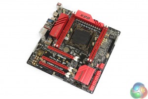
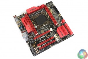
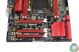
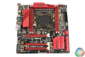
The ASRock X99M Killer uses the tried-and-tested black and red colour scheme. Feedback on our Facebook page suggests that many users are getting rather tired of the combination, although it is undeniably effortless to match with other components.
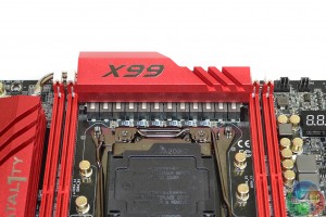
A pair of large aluminium alloy VRM heatsinks engulf a sizeable proportion of the motherboard's upper half. The cooling blocks were hot to the touch when the system was loaded, implying that they are doing a good job at removing heat from the stressed VRM components.
ASRock’s use of a true black PCB (rather than a washed out brown) is positive, and to be expected for a motherboard in this price range.
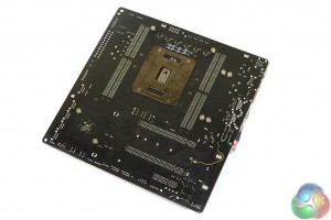
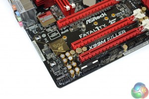
Rear-side solder points indicate the PCIe 3.0 distribution, with a full set of sixteen lanes being delivered to the first and second full-length slots. Four lanes are given to the third PCIe slot, making it more suited for a supplementary device (such as a PCIe SSD) than a graphics card.
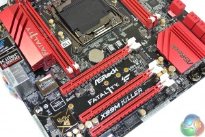
The LGA 2011-3 socket nestles between four DDR4 DIMM slots. Clearance is tight, so don’t expect to fit oversized memory modules under a large CPU cooler. We didn’t have interference worries with the potent VRM heatsinks – they’re short enough to be unobtrusive and do a good job at taking heat away from the hard-working MOSFETs.
Up to 32GB of DDR4 memory (using currently available 8GB consumer DIMMs) can be installed in the board. ASRock quotes supported frequencies of 3000MHz and above, which we will test later in the review.
ASRock deploys a twelve-phase power delivery system to feed the hungry Haswell-E CPUs. Management is conducted by Intersil's ISL6379 PWM controller, which is used extensively across ASRock's recent motherboards and seems to be receiving solid feedback amongst the enthusiast crowd.
Six phase doublers take the six lanes output by the ISL6379 controller and duplicate them into twelve links for the electronic components. This results in the twelve-phase system which is driven by six controller channels. The physical electronic components include 60A chokes, Fairchild FDMS3660S MOSFETs, and 12K-rated ‘Platinum' capacitors.
Two controllers marked MPDK 8632 cater for the memory and accompanying system voltage control. Dual-N MOSFETs are used for power switching in the memory subsystem.
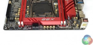
Two CPU fan headers and the 8-pin power connector are found along the board’s top edge. Straightforward access to the CPU power connector is provided by means of indenting half of the VRM heatsink.
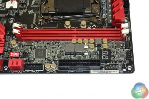
Called Dr Debug, a two-digit LED display is located close to the 24-pin power connector. I strongly believe that a debug display is a must on any overclocking motherboard – the assistance it provides when troubleshooting is convenient.
On one side of the 24-pin connector is an outwards-facing USB 3.0 header that gets its ports from the X99 chipset. ASRock places the TPM header on the other side, in one of the most bizarre locations that I have seen it in.
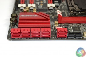
Ten right-angled SATA 6Gbps ports are located in the motherboard’s bottom-right corner. All ten of the ports operate directly from the X99 chipset, although Intel’s current design only permits the first six to be used for RAID. The remaining four should be reserved for slower mechanical storage, where possible.
The HDD Saver connector is situated behind the right pair of SATA ports. Gamers may find use from the ability to power down certain hard drives when they are not being accessed.
There is no SATA Express connector, although I do not see this as negative. M.2 is taking clear control of the high-speed (PCIe-fed) storage arena, leaving good ‘ol SATA 6Gbps perfectly capable of managing large storage drives. SATA Express, in its current form, is either deemed too bulky or too slow for many consumer applications (although that could change in the future).
A realistic usage scenario is likely to be two-card SLI and CrossFire. ASRock leaves a 1-slot gap between both of its high-bandwidth PCIe connections. This move provides dual-card support in mATX cases with four expansion slots, but it also means that the graphics boards will be back-to-back.
A 40-lane CPU feeds both of the upper slots with a full sixteen-lane PCIe 3.0 connection. The second slot is dropped to eight PCIe 3.0 lanes when a 28-lane CPU is installed. Both x16/x16 and x16/x8 configurations are perfectly capable of powering two graphics cards, with almost immeasurable performance differences existing between the two setups.
That third PCIe slot is physically wired with four lanes of connectivity, and ASRock routes those from the X99 chipset’s PCIe 2.0 stash. I don’t have many complaints about this decision – many devices expected to go inside a gaming PC, which aren’t graphics cards, are likely to be happy enough with the 20Gbps of bandwidth provided.
Where the decision does cause a lack of flexibility is for dual-card users who have a mATX chassis with five expansion slots. A preferable arrangement for those people would be to use the first and bottom PCIe slots for SLI/CrossFire, leaving a cooling gap between the consecutive boards. With a lane switching controller between the second and third PCIe slots, that would have been possible and would have provided an extra usable slot alongside two graphics cards. But with the lowest slot’s physical wiring of four lanes from the chipset, dual graphics cards must be positioned back-to-back, without any additional PCIe devices installed.
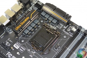
Another smart move would have been to add a non-intrusive mini-PCIe (or M.2) slot that could be used with internal wireless adapters. Gigabyte pulled this trick off to great effect with its X99M-Gaming 5.
ASRock’s Ultra M.2 slot provides a connection speed of up to 32Gbps via four lanes of PCIe 3.0 connectivity. And there is not any interference with the graphics subsystem’s lanes, so running PCIe 3.0 x4 M.2 can be done in addition to CrossFire or SLI on 40- and 28-lane CPUs.
There’s also capacity to install M.2 SATA SSDs in the slot, although that will render one of the ‘non-RAID’ SATA 6Gbps ports unusable.
Drive length support is a positive for ASRock’s implementation. While the 80mm-long M.2 2280 version is currently the most common form factor, support for up to 110mm-long drives provides future flexibility.
Along the bottom edge we see the usual affair of front panel headers. Audio is found to the left, the shortest signal distance from its related hardware, while the front panel chassis connectors reside to the right.
Other features of note are the two USB 2.0 headers, a downwards-facing molex power connector for beefy graphics configurations, and onboard power and reset buttons. ASRock certifies its Thunderbolt header for use with add-in cards.
ASRock's Purity Sound 2 audio system is based around the Realtek ALC1150 codec. Nichicon Fine Gold series capacitors smooth the audio signal while a pair of Texas Instruments NE5532 amplifiers cater for high impedance headphones.
A dedicated cover for the codec and a segregated audio path aim to minimise the level of EMI.
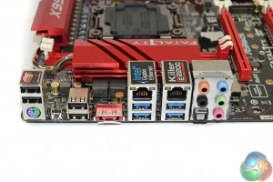
Four USB 3.0 ports and a further four USB 2.0 connectors are provided on the rear IO. All of the ports operate directly from the X99 chipset, and one of the USB 2.0 connections is given ASRock’s Fatal1ty mouse port capabilities.
A PS/2 port may please users interested in maximum compatibility, while the rear-mounted clear CMOS button is universally adored by overclockers who use a chassis. The eSATA 6Gbps port shares its connection with one of the ‘non-RAID’ internal connectors, meaning that only one can be used at any times.
ASRock clearly states which of the LAN ports is provided by the Killer E2200 NIC and Intel’s I218-V chipset. Killer’s NICs seem to separate gaming enthusiasts – some people like them while others call them a waste of money. By that logic, the inclusion of Intel and Killer NICs is smart on ASRock’s part, although it does undeniably add to the X99M Killer’s retail price. That will almost certainly be considered a waste of money by a greater proportion of gamers.
ASRock's fan header distribution is about as good as it gets for a micro-ATX motherboard. Two headers (one 4-pin and one 3-pin) cater for the CPU cooler, while a further three connectors (two 3-pin and one 4-pin) are evenly spread around the board.
Management duties are the task of Nuvoton's widely-used NCT6791D controller.
Dual BIOS chips are provided for redundancy purposes. Both of the socketed chips, and their associated switch, are situated below the CPU socket, making them easily accessible with a graphics card and not-too-big CPU cooler installed.
 KitGuru KitGuru.net – Tech News | Hardware News | Hardware Reviews | IOS | Mobile | Gaming | Graphics Cards



Did you ever get the RAM issue with reboots with high speeds sorted? I am having the same issue, although when my PC reboots it doesn’t fail to start up, but with tight timings on my current 16GB set (CL12@2666) or high speed (CL14@3200Mhz) I can’t get the PC to stay turned off, but other than that the RAM runs fine for day to day use if I keep the computer turned on. I am on the latest 3.30 BIOS revision as well.
Thanks
You’d probably be better off with the newer USB 3.1 revision of the board, it has the OC Socket with extra pins and is way better for RAM, especially overclocking.
Thanks for the reply! I may look into that, but not really in a position to replace the motherboard. It’s been a little over a year since buying. Wonder if they could offer some form of trade-in for this issue since it does look like a BIOS bug/glitch? Or I would probably assume this would fall under a clause of, “Not officially supported RAM, so nothing we can do”. Anyone have any experience working with ASRock on these kind of issues?
I bought exactly the same setup 2 years ago. The the Asrock F-Streaming overclocking software could not get a stable result. Not even at 4.0ghz. Read the article and emulated your 4.6ghz settings at 1.36v. Stable as a rock. Ended up at 1.33v. Below that it becomes unstable. Aircooled (noctua NH-D14) never get’s above 60c under load and idles around 25-30c. Was thinking about getting a 7700k but there’s no need for that now. Thanks.