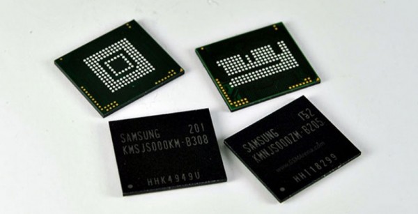
Samsung has announced this week that it has begun the mass production of its 4GB DRAM based on the HBM2 interface. These chips will be used in upcoming high-performance computing, advanced graphics and networking products and is said to be seven times faster than the current DRAM performance limit.
In a press release sent out today, Samsung explained that “By mass producing next-generation HBM2 DRAM, we can contribute much more to the rapid adoption of next-generation HPC systems by global IT companies”.
Samsung is using the 20nm process and HBM chip design for its 4GB DRAM chips and is specifically aiming these at graphics cards as well as HPC systems. Samsung even went ahead and explained how it created its new DRAM:
“The 4GB HBM2 package is created by stacking a buffer die at the bottom and four 8Gb core dies on top. These are then vertically interconnected by TSV holes and microbumps. A single 8Gb HBM2 die contains over 5,000 TSV holes, which is more than 36 times that of an 8Gb TSV DDR4 die, offering a dramatic improvement in data transmission performance compared to typical wire-bonding based packages.”
Samsung's HBM2 package features 256GB/s of bandwidth, which is double that of first-generation High-Bandwidth Memory. These new chips also bring enhanced power efficiency. While Samsung is producing 4GB DRAM chips right now, it will be moving on to 8GB versions later on in the year. According to Samsung, by using its 8GB HBM2 chips on graphics cards, designers will be able to save on 95 percent space compared to traditional GDDR5.
KitGuru Says: Samsung has kicked off mass production of HBM2 and hopefully by the summer, we'll have some graphics cards on the market to take advantage of it.
 KitGuru KitGuru.net – Tech News | Hardware News | Hardware Reviews | IOS | Mobile | Gaming | Graphics Cards


