Nvidia have experienced great success with their Maxwell architecture – cards such as the GTX750ti impressed my colleague Allan when he first analysed them back in February 2014. At prices around £100 the GTX 750ti firmly targeted the budget gamer working with a restrictive budget. If you have a bit more cash on hand then the recently announced GTX950 is priced between the GTX750ti and GTX960 – targeting AMD's R7 370. Today we look at the modified, highly overclocked Gigabyte GTX950 Xtreme Gaming partner card.
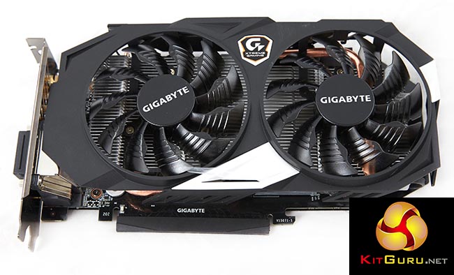
The Gigabyte GTX950 Xtreme Gaming 2GB incorporates dual, ridged fans with the company logo visible in the centre. The white racing stripe adds a bit of pizazz to the black.
| GPU | GeForce GTX 750 Ti (Maxwell) |
GeForce GTX 950 (Maxwell) |
GeForce GTX 960 (Maxwell) |
GeForce GTX 970 (Maxwell) |
GeForce GTX 980 (Maxwell) |
| GPU Codename | GM107 | GM206 | GM206 | GM204 | GM204 |
| Streaming Multiprocessors | 5 | 6 | 8 | 13 | 16 |
| CUDA Cores | 640 | 768 | 1024 | 1664 | 2048 |
| Base Clock | 1020 MHz | 1024 MHz | 1126 MHz | 1050 MHz | 1126 MHz |
| GPU Boost Clock | 1085 MHz | 1188 MHz | 1178 MHz | 1178 MHz | 1216 MHz |
| Total Video memory | 2GB | 2GB | 2GB | 4GB | 4GB |
| Texture Units | 40 | 48 | 64 | 104 | 128 |
| Texture fill-rate | 40.8 Gigatexels/sec | 49.2 Gigatexels/sec | 72.1 Gigatexels/sec | 109.2 Gigatexels/sec | 144.1 Gigatexels/sec |
| Memory Clock | 5400 MHz | 6600 MHz | 7010 MHz | 7000 MHz | 7000 MHz |
| Memory Bandwidth | 86.4 GB/sec | 105.6 GB/sec | 112.16 GB/sec | 224 GB/s | 224 GB/sec |
| Bus Width | 128bit | 128bit | 128bit | 256bit | 256bit |
| ROPs | 16 | 32 | 32 | 56 (following correction) |
64 |
| Manufacturing Process | 28nm | 28nm | 28nm | 28nm | 28nm |
| TDP | 60 Watts | 90 Watts | 120 Watts | 145 Watts | 165 Watts |
On a technical level, the cut-down iteration of the GM206 GPU is, in many areas, effectively 75% of the core used on a GTX 960. The GTX 950 version of the GM206 GPU ships with 768 CUDA cores and 48 texture units. Those numbers are more closely aligned with the GTX 750 Ti version of Nvidia’s first-gen Maxwell GM107 core, however specifically focusing on the number of ROPs puts clear daylight between the GTX 950 and its lower-end sibling.
The same 128bit memory interface found on the GTX 960 is present, however that may be less of a potential choking point given the reduced raw horsepower of the GTX 950’s cut-down GPU. As was the case with the GTX 960, the same argument for more efficient utilisation of the GM206’s 128bit memory interface, in comparison to Kepler, is made by Nvidia.
Clock speeds for the GTX 950 are sliced by comparison to GTX 960 frequencies. The reference core clock is rated at 1024MHz, with a maximum boost speed of 1188MHz. The 2GB of GDDR5 memory is rated to run at 1650MHz (6.6Gbps effective) to produce a bandwidth level of 105.6GB/sec. With that said, most board partners will be unlocking the GM206 core’s overclocking potential and shipping their cards with higher, factory-overclocked frequencies. Gigabyte are a case in point today, for instance.
Extending to the GTX 950’s features, the card supports the DirectX 12 API at feature level 12.1. A H.265 (HEVC) encoder/decoder engine built into the GPU, along with HDMI 2.0, shout loudly for the GTX 950 to be used inside a gaming HTPC. With the 90W TDP being low enough to comfortably fit inside SFF cases, the ability to output 60Hz video to a 4K TV (most of which do not have DisplayPort connections) is an important feature. HDMI 2.0 is a feature that team red’s competitor card cannot offer.
One of the more notable changes between the GTX 75x cards and the GTX 950 is the TDP differential. While the GTX 750 Ti had a 60W TDP, the GTX 950 ups that number to 90W. Approximating TDP as an indicator of power consumption, the 90W rating narrowly tips the GTX 950 into a region where it requires a 6-pin PCIe power connector. This emphasises that Nvidia is focused on gaming performance with its new card, while the GTX 750 Ti, for example, still remains to cater for those wanting a graphics card to run on a PSU without a 6-pin PCIe cable.
 KitGuru KitGuru.net – Tech News | Hardware News | Hardware Reviews | IOS | Mobile | Gaming | Graphics Cards


