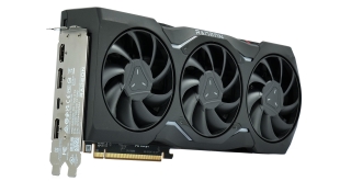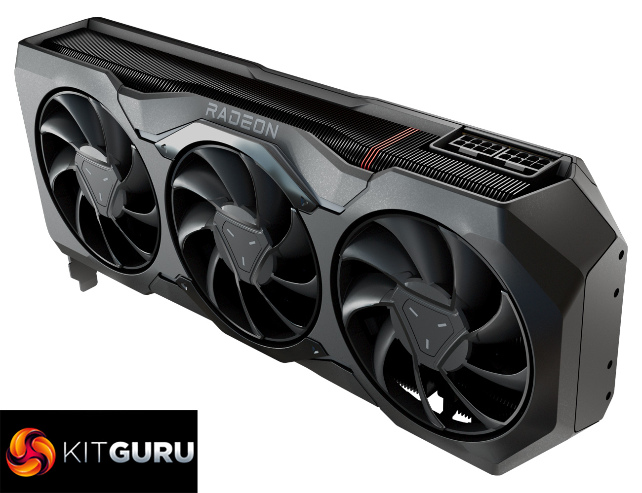
We have been eager to get hands on with the RX 7900 XTX ever since it was officially announced last month at AMD's event in Las Vegas. Priced at £999.99, this new flagship graphics card promises to outperform the more expensive RTX 4080 in rasterised games, while AMD also claims competitive ray tracing performance. Today we put the 7900 XTX through its paces and find out exactly how fast this GPU really is.
Following in the footsteps of the successful RDNA 2 architecture, AMD's new RX 7900 series products are built on RDNA 3, utilising the world's first chiplet-based gaming GPUs. The Radeon RX 7900 XTX is the company's new flagship, promising high performance at a lower price than the previous RX 6950 XT.
AMD is keen to emphasise improvements in power efficiency too, with a claimed 54% increase in performance per Watt versus RDNA 2. We know that Nvdia's Ada Lovelace architecture is itself highly efficient so it will be interesting to see how the RX 7900 XTX compares.
It's also worth noting that while this is a standalone review for the RX 7900 XTX, we do also have a day one review for the RX 7900 XT, and you can find that HERE.
If you want to read this review as a single page, click HERE.
| RX 7900 XTX | RX 7900 XT | RX 6950 XT | RX 6900 XT | RX 6800 XT | RX 6800 | |
| Architecture | RDNA 3 | RDNA 3 | RDNA 2 | RDNA 2 | RDNA 2 | RDNA 2 |
| Manufacturing Process | 5nm GCD + 6nm MCD | 5nm GCD + 6nm MCD | 7nm | 7nm | 7nm | 7nm |
| Transistor Count | 57.7 billion | 57.7 billion | 26.8 billion | 26.8 billion | 26.8 billion | 26.8 billion |
| Die Size | 300 mm² GCD 220 mm² MCD | 300 mm² GCD 220 mm² MCD | 519 mm² | 519 mm² | 519 mm² | 519 mm² |
| Ray Accelerators | 96 | 84 | 80 | 80 | 72 | 60 |
| Compute Units | 96 | 84 | 80 | 80 | 72 | 60 |
| Stream Processors | 6144 | 5376 | 5120 | 5120 | 4608 | 3840 |
| Game GPU Clock | Up to 2300MHz | Up to 2000 MHz | Up to 2100MHz | Up to 2015MHz | Up to 2015MHz | Up to 1815MHz |
| Boost GPU Clock | Up to 2500 MHz | Up to 2400 MHz | Up to 2310MHz | Up to 2250MHz | Up to 2250MHz | Up to 2105MHz |
| ROPs | 192 | 192 | 128 | 128 | 128 | 96 |
| AMD Infinity Cache | 96MB | 80MB | 128MB | 128MB | 128MB | 128MB |
| Memory | 24GB GDDR6 | 20GB GDDR6 | 16GB GDDR6 18Gbps | 16GB GDDR6 16Gbps | 16GB GDDR6 | 16GB GDDR6 |
| Memory Bandwidth | 960 GB/s | 800 GB/s | 576 GB/s | 512 GB/s | 512 GB/s | 512 GB/s |
| Memory Interface | 384-bit | 320-bit | 256-bit | 256-bit | 256-bit | 256-bit |
| Board Power | 355W | 315W | 335W | 300W | 300W | 250W |
First, let's take a quick look at the specs. We've already covered the key figures in our announcement article, but it's worth recapping the core details here.
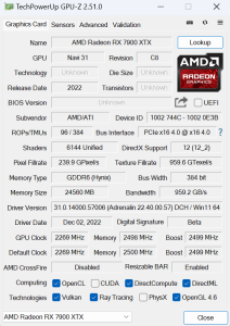
For starters, the RDNA 3 architecture has seen AMD transition to a chiplet-based design – a world first for a gaming GPU. We find a 300mm² Graphics Compute Die, based on TSMC's 5nm node, flanked by six 37mm² Memory Cache Dies. In total, the Navi 31 GPU packs 57.7 billion transistors.
Internally, the GCD makeup hasn't been radically changed compared to what we saw with RDNA 2. That means Navi 31 packs in 96 Compute Units, each of which houses 64 Steam Processors, for a total of 6144 shaders. There's also 96 Ray Accelerators – one per CU – and 192 ROPs.
As for clock speed, AMD has de-coupled the clocks, so the front-end and shaders can operate at different clock speeds in a bid to save power. With the RX 7900 XTX, the shader clock features a rated game clock of up to 2300MHz, and a boost of up to 2500MHz.
Meanwhile, the memory configuration has taken a step forward. The RX 7900 XTX packs 24GB of GDDR6 memory clocked at 20Gbps, operating over a 384-bit memory interface, for total memory bandwidth of 960 GB/s. 96MB of Infinity Cache is also present, which allows AMD to claim an ‘effective memory bandwidth' of up to 3500 GB/s.
Power draw for the RX 7900 XTX is rated at 355W Total Board Power (TBP), but we are using our updated GPU power testing methodology in this review, so read on for our most detailed power and efficiency testing yet.
 KitGuru KitGuru.net – Tech News | Hardware News | Hardware Reviews | IOS | Mobile | Gaming | Graphics Cards


