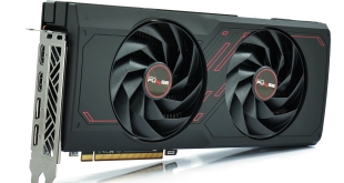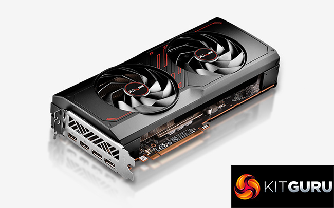
Less than two weeks on from their announcement at Gamescom 2023, today marks the release of AMD's new mid-range GPUs, the RX 7700 XT and the RX 7800 XT. This review will focus on the former card, though we do have a separate analysis of the RX 7800 XT if you want to read that. Utilising a cut-down implementation of AMD's Navi 32 chiplet-based silicon, the RX 7700 XT lands at £429.99, with AMD positioning it head-to-head against the RTX 4060 Ti 16GB. Today we find out which of these mid-range GPUs will come out on top…
Unlike the RX 7800 XT, which isn't necessarily a direct successor to the RX 6800 XT, AMD's new RX 7700 XT is a clear continuation from the RX 6700 XT. Both launched at around the same price, with the RX 7700 XT just £10 more expensive in terms of MSRP, while they both slot neatly into the mid-tier of AMD's existing offerings.
Despite the RTX 4060 Ti 16GB initially launching at £479, cards are already available at just £430, making this a straight shoot-out between the two GPUs. We test twelve games, plus another eight with ray tracing enabled, while also focusing on power draw and efficiency in today's review.
If you want to read this review as a single page, click HERE.
| RX 7900 XT | RX 7800 XT | RX 7700 XT | RX 6800 XT | RX 6800 | RX 6700 XT | |
| Architecture | RDNA 3 | RDNA 3 | RDNA 3 | RDNA 2 | RDNA 2 | RDNA 2 |
| Manufacturing Process | 5nm GCD + 6nm MCD | 5nm GCD + 6nm MCD | 5nm GCD + 6nm MCD | 7nm | 7nm | 7nm |
| Transistor Count | 57.7 billion | 28.1 billion | 28.1 billion | 26.8 billion | 26.8 billion | 17.2 billion |
| Die Size | 300 mm² GCD
220 mm² MCD |
200 mm² GCD
150 mm² MCD |
200 mm² GCD
150 mm² MCD |
519 mm² | 519 mm² | 336 mm² |
| Compute Units | 84 | 60 | 54 | 72 | 60 | 40 |
| Ray Accelerators | 84 | 60 | 54 | 72 | 60 | 40 |
| Stream Processors | 5376 | 3840 | 3456 | 4608 | 3840 | 2560 |
| Game GPU Clock | Up to 2000 MHz | 2124 MHz | 2171 MHz | Up to 2015MHz | Up to 1815MHz | Up to 2424MHz |
| Boost GPU Clock | Up to 2400 MHz | Up to 2430 MHz | Up to 2544 MHz | Up to 2250MHz | Up to 2105MHz | Up to 2581MHz |
| ROPs | 192 | 96 | 96 | 128 | 96 | 64 |
| AMD Infinity Cache | 80MB | 64MB | 48MB | 128MB | 128MB | 96MB |
| Memory | 20GB GDDR6 20Gbps | 16GB GDDR6 19.5 Gbps | 12GB GDDR6 18Gbps | 16GB GDDR6 16Gbps | 16GB GDDR6 16Gbps | 12GB GDDR6 16Gbps |
| Memory Bandwidth | 800 GB/s | 624 GB/s | 432 GB/s | 512 GB/s | 512 GB/s | 384 GB/s |
| Memory Interface | 320-bit | 256-bit | 192-bit | 256-bit | 256-bit | 192-bit |
| Board Power | 315W | 263W | 245W | 300W | 250W | 230W |
First, let's take a quick look at the specs. Unlike the most recent RDNA 3 GPU – the RX 7600 – AMD has made a return to its chiplet-based design for the RX 7700 XT, as we initially saw last year with the RX 7900 XTX and 7900 XT. This time around, the 7700 XT offers a 200mm² Graphics Compute Die (GCD) using TSMC's 5nm process, flanked by four 150 mm² Memory Compute Dies (MCDs) built on TSMC's 6nm node. One of those MCDs is disabled however, as the 7700 XT is not a full implementation of Navi 32.
Internally though, the compute makeup hasn't been radically changed. The cut-down Navi 32 silicon deployed here packs in 54 Compute Units, each of which houses 64 Stream Processors, for a total of 3456 shaders. There's also 54 Ray Accelerators – one per CU – and 96 ROPs.
As for clock speed, this remains high with the RX 7700 XT, with AMD touting a boost of up to 2544MHz, though a slightly lower game clock of 2171MHz.
Meanwhile, the memory configuration is almost identical to the previous generation RX 6700 XT. We still find 12GB GDDR6 operating over a 192-bit interface, but this time the memory clocks in at 18Gbps, up from 16Gbps. This gives a memory bandwidth of 432 GB/s, though AMD claims an ‘effective' bandwidth of 1995.3 GB/s due to the 64MB of 2nd Gen Infinity cache.
Power draw for the RX 7700 XT is rated at 245W Total Board Power (TBP), though AMD pointed out to us that this is an ‘up to' figure. We are using our well-established GPU power testing methodology in this review, so read on for our most detailed power and efficiency testing yet.
 KitGuru KitGuru.net – Tech News | Hardware News | Hardware Reviews | IOS | Mobile | Gaming | Graphics Cards


