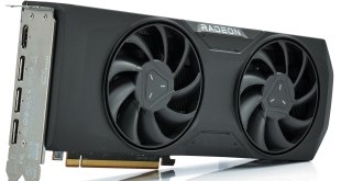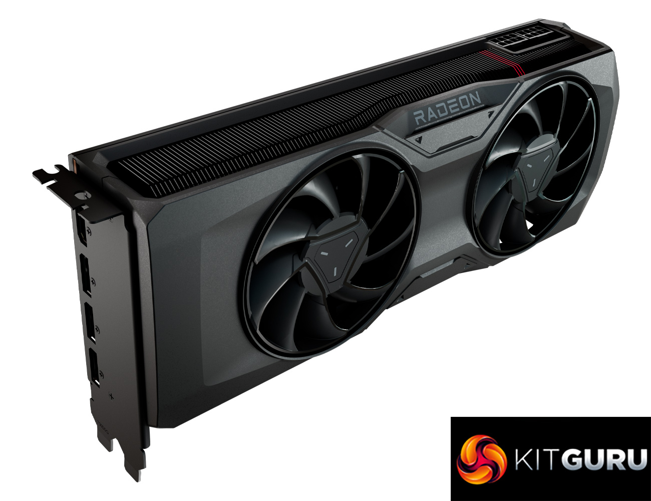
Hot on the heels of their announcement at Gamescom 2023, today marks the release of AMD's new mid-range GPUs, the RX 7700 XT and the RX 7800 XT. This review will focus on the latter model, though we do have a separate analysis of the RX 7700 XT if you want to read that. Built on new Navi 32 chiplet-based silicon, this graphics card hits the market at £479.99, and AMD claims it is faster than Nvidia's RTX 4070. We put it to the test over twelve games, plus another eight tested with ray tracing, to find out exactly how it performs… and yes, we did benchmark Starfield!
As with any new GPU launch, there is plenty to discuss today and we will cover as much as we can in this written article and in the video review embedded above. I do feel it is important to manage expectations for the RX 7800 XT, as I don't necessarily agree with the naming scheme. On paper, it sounds like the successor to the RX 6800 XT that launched back in November 2020, but the reality is the two products are positioned quite differently.
For one, the RX 7800 XT is launching at an MSRP of £479.99, £120 lower than the £599.99 launch price of the 6800 XT. The new GPU is also built on AMD's mid-range Navi 32 silicon and sits three models below the flagship 7900 XTX, whereas the 6800 XT used the biggest Navi 21 die and was positioned a single tier below the RX 6900 XT at launch. In actuality, the pricing and position of this RDNA 3 card would put it somewhere between the RX 6700 XT and RX 6800 – but let's see how things shake out in our benchmarks…
If you want to read this review as a single page, click HERE.
| RX 7900 XT | RX 7800 XT | RX 7700 XT | RX 6800 XT | RX 6800 | RX 6700 XT | |
| Architecture | RDNA 3 | RDNA 3 | RDNA 3 | RDNA 2 | RDNA 2 | RDNA 2 |
| Manufacturing Process | 5nm GCD + 6nm MCD | 5nm GCD + 6nm MCD | 5nm GCD + 6nm MCD | 7nm | 7nm | 7nm |
| Transistor Count | 57.7 billion | 28.1 billion | 28.1 billion | 26.8 billion | 26.8 billion | 17.2 billion |
| Die Size | 300 mm² GCD
220 mm² MCD |
200 mm² GCD
150 mm² MCD |
200 mm² GCD
150 mm² MCD |
519 mm² | 519 mm² | 336 mm² |
| Compute Units | 84 | 60 | 54 | 72 | 60 | 40 |
| Ray Accelerators | 84 | 60 | 54 | 72 | 60 | 40 |
| Stream Processors | 5376 | 3840 | 3456 | 4608 | 3840 | 2560 |
| Game GPU Clock | Up to 2000 MHz | 2124 MHz | 2171 MHz | Up to 2015MHz | Up to 1815MHz | Up to 2424MHz |
| Boost GPU Clock | Up to 2400 MHz | Up to 2430 MHz | Up to 2544 MHz | Up to 2250MHz | Up to 2105MHz | Up to 2581MHz |
| ROPs | 192 | 96 | 96 | 128 | 96 | 64 |
| AMD Infinity Cache | 80MB | 64MB | 48MB | 128MB | 128MB | 96MB |
| Memory | 20GB GDDR6 20Gbps | 16GB GDDR6 19.5 Gbps | 12GB GDDR6 18Gbps | 16GB GDDR6 16Gbps | 16GB GDDR6 16Gbps | 12GB GDDR6 16Gbps |
| Memory Bandwidth | 800 GB/s | 624 GB/s | 432 GB/s | 512 GB/s | 512 GB/s | 384 GB/s |
| Memory Interface | 320-bit | 256-bit | 192-bit | 256-bit | 256-bit | 192-bit |
| Board Power | 315W | 263W | 245W | 300W | 250W | 230W |
First, let's take a quick look at the specs. Unlike the most recent RDNA 3 GPU – the RX 7600 – AMD has made a return to its chiplet-based design for the RX 7800 XT, as we initially saw last year with the RX 7900 XTX and 7900 XT. This time around, the 7800 XT offers a 200mm² Graphics Compute Die (GCD) using TSMC's 5nm process, flanked by four 150 mm² Memory Compute Dies (MCDs) built on TSMC's 6nm node.
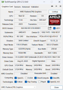
Internally though, the compute makeup hasn't been radically changed. Navi 32 packs in 60 Compute Units, each of which houses 64 Stream Processors, for a total of 3840 shaders. There are also 60 Ray Accelerators – one per CU – and 96 ROPs.
As for clock speed, this remains high with the RX 7800 XT, with AMD touting a boost of up to 2430MHz, though a slightly lower game clock of 2124MHz.
Meanwhile, the memory configuration is almost identical to the previous generation RX 6800 XT. We still find 16GB GDDR6 operating over a 256-bit interface, but this time the memory clocks in at 19.5Gbps, up from 16Gbps. This gives a memory bandwidth of 624 GB/s, though AMD claims an ‘effective' bandwidth of 2708.4 GB/s due to the 64MB of 2nd Gen Infinity cache.
Power draw for the RX 7800 XT is rated at 263W Total Board Power (TBP), though AMD pointed out to us that this is an ‘up to' figure. We are using our well-established GPU power testing methodology in this review, so read on for our most detailed power and efficiency testing yet.
 KitGuru KitGuru.net – Tech News | Hardware News | Hardware Reviews | IOS | Mobile | Gaming | Graphics Cards


