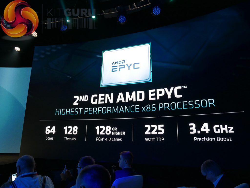
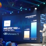
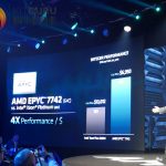
AMD has today officially launched its new range of Zen 2-based EPYC datacenter CPUs, codenamed Rome, introducing the world's highest performance x86 processor. Launching with several SKUs ranging from 8C16T models all the way up to the sixty-four core flagship, AMD is asserting what the company believes to be its position of dominance in terms of compute performance, efficiency, and security.
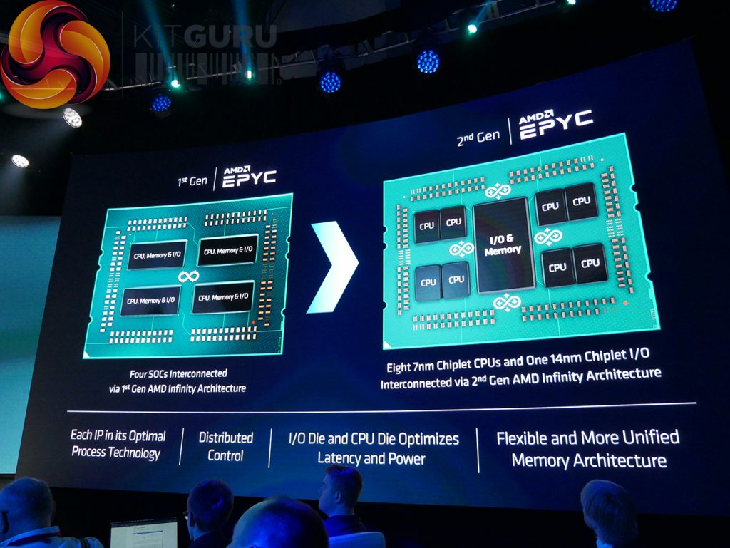
Based on AMD’s new Zen 2 architecture that we first saw deployed in the Ryzen 3000 series of consumer processors, EPYC Rome uses the same CCX and CCD design that is built upon TSMC’s 7nm FinFET process. The difference between those AM4 consumer chips that top out at sixteen cores and 32 threads comes most notably from the significant increase to core count thanks to AMD’s continued use of the hybrid multi-die approach. Up to eight CCDs, each of which features two CCXs with up to four cores and 16MB of L3 cache, can be positioned alongside a dedicated IO die to create a processor with up to 64 compute cores and up to 256MB of L3 cache.
Architectural improvements that we have already seen on Ryzen 3000 are present within EPYC Rome processors. AMD quotes 15% IPC improvement versus the previous generation, which has proven to be a fair claim based on Ryzen 3000 testing. Improvements brought about by the TAGE branch predictor are highlighted. Doubled floating point performance and a doubling of L3 cache per CCX are also important.
One of the most notable improvements which has proven successful on the consumer desktop is the enhanced AVX256 performance. The single-op 256-bit data path allows for improved performance in AVX-based workloads compared to the previous dual-op approach for the Zen architecture. This is of high importance to datacenter and HPC users with heavy AVX workloads as it is typically an area where Intel’s alternative implementation has proven to be successful, even despite the reduced turbo frequency bins under such scenarios. Combined with double the core count, the improved AVX architecture for Zen 2 EPYC provides 4x the floating point performance, which is key for many dynamic modelling workloads.
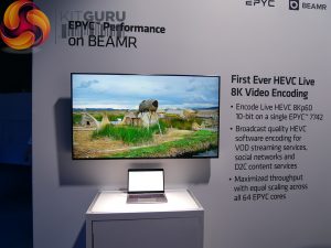
We saw an example from video technology company Beamr whereby extremely high bitrate 8K60 HDR video footage was being processed down to 50Mbps using the HEVC codec. This was being run on the 64-core EPYC 7742 and had the processor running close to maximum utilisation across all cores. Asked whether this workload would run on previous generation EPYC CPUs, all of which have the inherent design disadvantage in terms of AVX performance, the answer was a convincing ‘no'. Multiple 4K streams were the maximum capability for those chips, compared to the single 8K60 stream we saw on show.
Power efficiency can be critical here, especially for live sports events being shot in high resolution and at high frame rates. At-the-event compute capability is required to process the high bitrate data down to a lower bitrate using a mezzanine codec where it can be more easily satellite streamed to the next step of the process. The reduction in electrical power requirements for this compute task is important, with live sports setups often being positioned in trucks at the stadium whereby plentiful power is not so easily attainable as it is inside a datacenter. That's the power of 7nm and the efficiency it provides Zen 2 processors.
Continuing the 7nm focus, Chief Architect of Cores at AMD – Mike Clark – was keen to point out the benefits that TSMC’s process node provides AMD. 7nm FinFET technology drives possibilities such as 2x density, greater than 1.25x frequency for the same power, or half the power for the same performance versus previous generations. To datacenter operators with an eye on performance per Watt and compute performance density, those three points are critical to business profitability through the potential to reduce operational expenditure and therefore TCO. Being able to squeeze more cores into a single box compared to previous generation EPYC and also Intel competition is important. It reduces the overhead necessitated by additional non-compute hardware in increased numbers of servers which can be perceived as dead money. That can help to reduce capital expenditure, which also plays a big part in the TCO equation.
Interestingly, one of AMD's slides was particularly honest in comparing its perception of its process technology compared to Intel’s. AMD highlights the performance per Watt advantage for Intel’s 14nm and 14nm+ process nodes versus Global Foundries 14nm and 12nm technology. The leapfrog occurs with the transition to TSMC’s 7nm FinFET processor node – a manufacturing node that AMD is confident will give it a performance per Watt advantage even versus Intel's 10nm process.
AMD was keen to highlight how the number of CCDs used can be tweaked to their preference for market segmentation. Cores can also be disabled and fused off in conventional manners to create niche processors for specific target audiences, such as an eight-core, sixteen-thread part with a hefty 128MB of L3 cache.
Unlike previous EPYC processors, which were effectively four Ryzen 7 processors on a single substrate linked together via Infinity Fabric, EPYC Rome is slightly different in how it scales compared to Ryzen. Instead, the IO die is created specifically for EPYC and is fabbed on a 14nm process node.
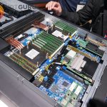
Arguably most notable within the IO die is the memory controller. Eight channel DDR4, with up to 2 DIMMs per channel, is supported. This time, however, frequency capability comes in at 3200MHz, albeit in a 1 DIMM per channel configuration. Speaking to a Microsoft Azure engineer, the preferred implementation for many latency-sensitive workloads will be in a 1 DIMM per channel DDR4-3200 configuration. With the availability of high capacity DIMMs, this still permits high memory capacities whilst also avoiding the potential reduction to around DDR4-2400 frequency, memory controller dependent, with a 2 DIMM per channel configuration.
Crunching the numbers, AMD quotes memory capacity for up 4TB of RAM per single socket CPU. That's a notable increase compared to the Intel competition where users would be required to go down a multi-socket approach to reach such RAM capacities in a single server. Workloads that benefit from high quantities of system memory, such as virtualisation and certain simulation solvers, can benefit from hordes of system memory without users being forced to over-purchase on the CPU compute capability or deal with the overheads of a multi-socket motherboard.
Also critical to IO capability is the PCIe lane capacity. Each single CPU offers 128 PCIe Gen 4 lanes, with bifurcation allowing up to 8 devices per 16-lane link. The increased bandwidth permitted for high-speed storage is a key benefit that PCIe Gen 4 brings to the market. Big data or other workloads that heavily interact with high capacity flash storage can benefit from the faster speeds to the storage infrastructure. The same higher-bandwidth Gen 4 benefits can be important in GPU compute scenarios whereby data can be frequently shifting between high performance compute cards and accelerators.
AMD highlights how up to 162 PCIe Gen 4 lanes can be provided by a single dual-socket EPYC Rome system. The CPU-to-CPU interaction doesn't permit for a full 100% increase in available PCIe lanes versus a single socket system. AMD does, however, allow for an additional 16 lanes per CPU to be carved off and added to the total pool. Some other resources can be reallocated, thus taking the total PCIe Gen 4 capacity to a possible 162 lanes.
Security is an area that AMD has put particular emphasis on. Built in to the processor is a discrete AMD secure processor that can handle certain security operation in isolation from the main x86 CPU. This can help to minimise possible attack vectors and the ability to attack the AMD secure processor via the main x86 CPU, in theory. Memory encryption is one particular area that AMD highlighted. Secure Memory Encryption (SME) limits the ability of the hypervisor administrator to view data being shifted through memory in the managed VMs. This is particularly important in scenarios such as web servers whereby sensitive user information, such as names and addresses, can be shifted through memory.
Secure Encrypted Virtualisation (SEV) is another piece of the security puzzle. The implementation allows for individual VMs to be isolated. Importantly, this helps to eliminate (perhaps mitigate is a more reasonable term) the possibility for administrator tampering and it helps to protect against an untrusted hypervisor. One key per VM and one key per hypervisor helps to protect VMs from one another and it also means that the hypervisor only has limited control over the VM and therefore is a less useful attack vector. Another area managed by the AMD secure processor are the encryption keys for the AES-128 engine in the memory controller.
Top of the performance stack is AMD's flagship EPYC 7742 processor. This is a 64-core, 128-thread CPU with a TDP of 225W. AMD allows the TDP to be configured up to 240W, if a hardware vendor builds the cooling and power delivery capacity for such an increase. With 8 CCDs and therefore 16 CCXs deployed, the flagship gets 256MB of L3 cache, giving dual-socket users a huge half-a-Gigabyte of L3 cache capacity. That's in addition to 8-channel DDR4-3200MHz capacity with up to 4TB of system RAM support (albeit at reduced frequencies in 2 DPC mode). 128 PCIe Gen 4 lanes are provided.
Clock speeds are 2.25GHz base and up to 3.4GHz boost. AMD highlighted how the clock speed is dependent upon the number of cores loaded, not the workload as we see with Intel’s AVX offset. Reading from AMD's graph, it looks like 1-8 core loads will run at 3.4GHz, 16-core loads see a drop to around 3.325GHz, 32-core loads drop to around 3.275GHz, and 48-64 core loads deliver 3.2GHz.
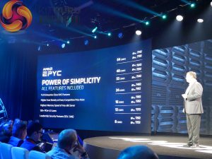
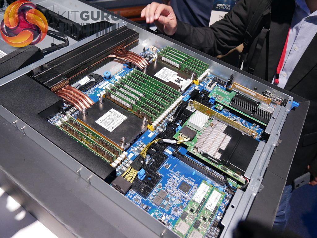
Additional options in the product stack include 8, 12, 16, 24, 32, and 48 core processors. Some single-socket-only options are also available for a pure market segmentation purpose – the multi-socket linkage hardware is fused off to save resources. Each processor offers 128 PCIe Gen 4 lanes and eight-channel memory capacity thanks to the dedicated IO die that is physically isolated from the core dies. As we have seen with the consumer AM4 platform, Zen 2-based EPYC processors can be dropped into Zen 1-based motherboards with a software update. This is perhaps important for smaller server users who wish to use some of the performance upgrades that Zen 2 provides without having to negotiate with purchasing departments for the sizeable outlay of a brand new server.
AMD is clearly optimising the product stack based on specific usage scenarios. For example, there's an 8-core EPYC 7262 processor that features 128MB of L3 cache – double that of other 8/12/16-core models. That increased cache capacity comes through the use of eight CCXs, albeit with 3 cores per 4-core CCX disabled. At 155W TDP and 180W cTDPMax, the heightened TDP number implies that lesser quality silicon is being used for this specific SKU. However, that may be of little downside to specific market segments that require high cache capacity without the associated core count, such as specific software engineering and programming workloads.
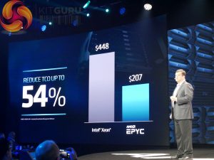
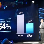
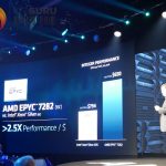
AMD's Zen 2-based EPYC Rome processors are shipping as of July 2019. Partners include Dell-EMC, Hewlett Packard Enterprise, and Google, to name just a few. It will be interesting to see how Intel's 56-core Xeon Platinum processors will compare against the 64-core AMD EPYC 7742 flagship. Although pricing information is heavily driven by supplier configurations, the real competitor to the 64-core EPYC 7742 looks to be Intel's Xeon Platinum 8200 series processors, not the 9200 series. With Intel's common Cascade Lake processors topping out at 28 cores and with a price tag sometimes over $10,000 per CPU, AMD is keen to pitch EPYC Rome as offering higher compute capability through increased core counts and lower TCO through drastically reduced asking prices.
KitGuru Says: Do you think that AMD's scalable approach to its 7nm Zen 2-based processors will prove highly successful with EPYC 7002 series and steal market share from Intel? Comment below.
 KitGuru KitGuru.net – Tech News | Hardware News | Hardware Reviews | IOS | Mobile | Gaming | Graphics Cards


