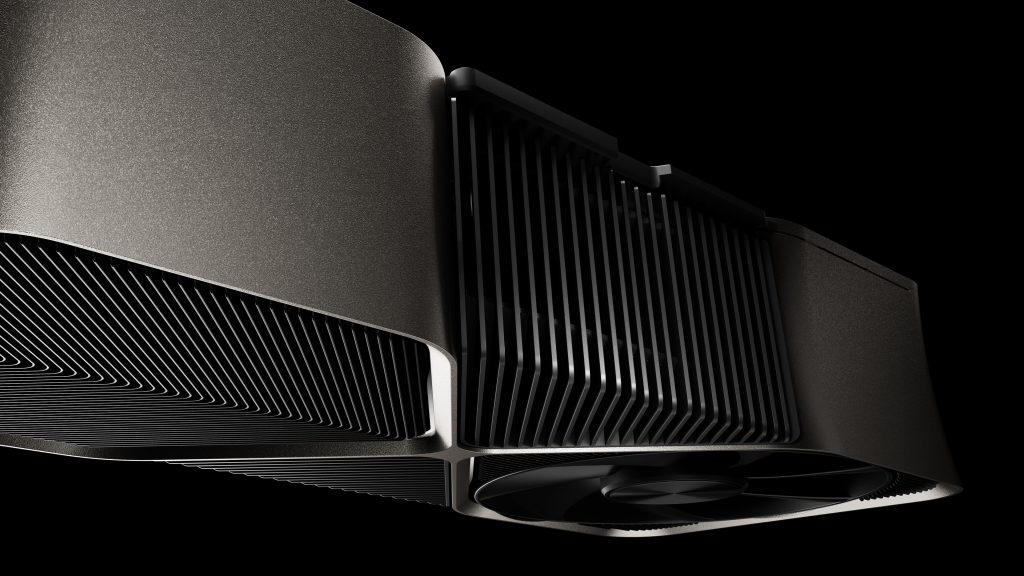
A leaked image of an Nvidia GeForce RTX 5090 PCB has surfaced online, offering a glimpse into the architecture of Nvidia's next-generation flagship graphics card.
The image shared on Chiphell (via HXL) showcases a large PCB, significantly larger than typical designs, packed with over 40 capacitors and a massive package substrate for the GPU. Previous reports claimed that the GPU would measure 24×31 mm with a package size of 63×56 mm, which seems to match the photo.
The photo also shows 16 slots for VRAM modules. The arrangement of the VRAM modules matches previously leaked information, with five modules on each side, four on top, and two below the GPU. This configuration could support various memory capacities, ranging from 32GB to 64GB, depending on the memory modules' density (2GB, 3GB, or 4GB). The PCB also features a single power connector, likely the new 12VHPWR (12V-6×2) connector designed for high-power GPUs. Moreover, the photo shows the card uses a PCIe 5.0 interface, as seen by its interface pattern.
While the lack of visible Nvidia branding suggests this isn't a Founders Edition card, a closer examination of the PCB reveals that this is a PNY sample based on the PG145 board and the GB202 GPU.
Nvidia is expected to unveil the RTX 5090 and other RTX 50 series GPUs at its keynote at CES 2025.
KitGuru says: With such a massive PCB, we wonder how big the final product will be. If you plan on getting an RTX 5090, know that you might have to change your case, or this behemoth might not fit.
 KitGuru KitGuru.net – Tech News | Hardware News | Hardware Reviews | IOS | Mobile | Gaming | Graphics Cards


